Understanding the Leakage Current Components in Short Channel MOS Transistors
This article covers the basics of MOS transistors with a view towards better understanding the leakage current that can occur in such transistors.
MOS transistors are getting scaled down to maximize their package density inside integrated circuits. This has led to the reduction of oxide thickness which, in turn, has reduced the threshold voltage of the MOS devices. At lower threshold voltages, leakage current becomes significant and contributes towards power dissipation. This is why it's vital that we know the various types of leakage currents in a MOS transistor.
Before we try to understand the various leakage current components, let's first revisit MOS transistor core concepts. This will help us gain better insights into the topic.
The MOS Transistor Structure Revisited
The MOS transistor structure consists of a metal, an oxide, and a semiconductor structure (hence, MOS).
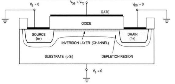
Consider an NMOS transistor with p-substrate and n+ diffusion wells as drain and source terminals. The oxide layer is made of SiO2 and is grown over the channel between the drain and source. The gate terminal is made of n+ doped polysilicon or aluminum.

Figure 1. The bird’s eye view of an NMOS transistor. All images from S. M. Kang, Y. Leblebici, CMOS Digital Integrated Circuits, TMH, 2003, ch.3, pp:83-93
In unbiased condition, the pn junctions at the drain/source and substrate interface are reverse biased. The energy band diagram of the transistor is as shown in Figure 2.

Figure 2. The energy band diagram of an unbiased NMOS transistor
As you can see, the Fermi levels of the metal, oxide, and semiconductor align themselves. There is a bend in the Si energy bands due to the voltage drop at the oxide-semiconductor interface. The direction of the in-built electric field is from metal to oxide to semiconductor and the direction of the voltage drop is opposite of the direction of the electric field.
This voltage drop occurs due to the work function difference between metal and semiconductor (part of the voltage drop takes place across the oxide and the rest across the Si-SiO2 interface). The work function is the amount of energy required for the electrons to escape from the Fermi level to free space. You can understand more about the MOS transistor band diagram and band bending in this video by Jordan Edmunds.
Accumulation
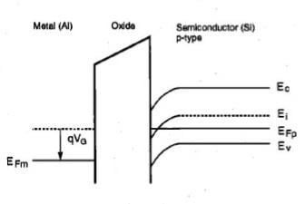
Next, suppose the gate has negative voltage and the source where the drain and the substrate are grounded. Due to the negative voltage, the holes in the substrate (majority carriers) are attracted to the surface. This phenomenon is called accumulation. The minority carriers in the substrate (electrons) are pushed back deep into it. The corresponding energy band diagram is given below.

Figure 3. The energy band diagram of an NMOS transistor with negative voltage on the gate terminal
Since the direction of electric field is from semiconductor to oxide to metal, the energy bands bend in the opposite direction. Also, notice the shifts in Fermi levels.
Depletion and Depletion Regions
Alternatively, consider the gate voltage to be just greater than zero. The holes are repelled back into the substrate and the channel is depleted of any mobile charge carriers. This phenomenon is called depletion and a depletion region wider than in the unbiased condition is created.

Figure 4. The depletion region in an NMOS

Figure 5. The corresponding energy band diagram for the NMOS depletion region shown in Figure 4
Since the electric field is from metal to oxide to semiconductor, the energy bands bend in the downward direction.
Surface Inversion
If the positive voltage at the gate is further increased, the minority carriers in the substrate (electrons) are attracted to the surface of the channel. This phenomenon is called surface inversion and the gate voltage at which the surface just inverts is known as threshold voltage (Vth).

Figure 6. Surface inversion in NMOS transistor

Figure 7. The corresponding energy band diagram for the NMOS transistor shown in Figure 6
The electrons create a conduction channel between the source and the drain. If the drain voltage is then increased from zero potential, a drain current (Id) starts flowing between the source and the drain. The energy bands bend further downwards and at the semiconductor-oxide interface.
Here, the intrinsic Fermi level is lesser than the Fermi level of a p-type substrate. This supports the point that, at the surface, the semiconductor is n-type (in the energy band diagrams of an n-type material, the intrinsic Fermi level is at a lesser energy level than the donor energy level).
In the next article, we'll delineate six types of leakage current found in MOS transistors.


