
Understanding ADC Integral Nonlinearity (INL) Error
Learn about the integral nonlinearity (INL) specification and how it relates to analog-to-digital converter (ADC) errors.
Three parameters, namely offset error, gain error, and INL, determine the accuracy of an ADC. Offset and gain errors can be calibrated out, which leaves us with INL as the main error contributor. The INL specification describes the deviation of the transition points of the actual transfer function from the ideal values.
What is Integral Nonlinearity (INL)?
An ideal ADC has a uniform staircase input-output characteristic, meaning that each transition occurs at 1 LSB (least significant bit) from the previous transition. However, with a real-world ADC, the steps are not uniform. As an example, consider the transfer curve shown in Figure 1.
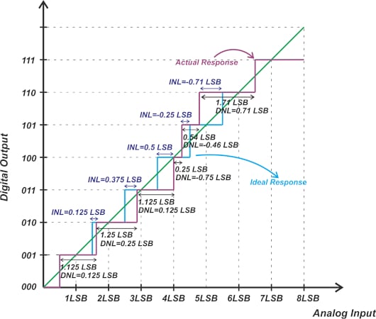
Figure 1. Example transfer curve for an ADC.
The deviation of a step width from the ideal value is characterized by the differential nonlinearity (DNL) specification. However, the DNL error cannot completely describe the transfer function deviation from the ideal response because the response we obtain depends on how the positive and negative DNL errors are spread across different codes. The INL specification allows us to characterize the deviation of code transitions from their ideal values. To calculate the INL of code k, we can use the following equation:
\[INL(k)=\frac{T_{a}(k)-T_{ideal}(k)}{Ideal \text{ } Step \text{ } Size}\]
Where Ta(k) and Tideal(k) respectively denote the actual and the ideal transition from code k-1 to k; and the “ideal step size” is the LSB of the ADC. For the above example, the actual transition from code 1 (001) to code 2 (010) occurs at 0.125 LSB above the ideal transition. Therefore, the INL of code 2 is INL(2) = +0.125 LSB.
From here, we might ask, what about the next transition (from code 2 to 3)? Noting that the transition from code 1 to 2 occurs at 0.125 LSB above the ideal value and taking into account that code 2 has a width error (or DNL) of +0.25 LSB, we can deduce that the transition from code 2 to 3 should occur at 0.375 LSB above the ideal value. Thus, we have INL(3) = +0.375 LSB. As you can see, the INL of code 3 is equal to the sum of the DNL of codes 1 and 2:
\[INL(3)=DNL(1)+DNL(2)=+0.125 \text{ } LSB +0.25 \text{ } LSB = +0.375 \text{ } LSB\]
Extending the above analysis to the other codes, it is easy to verify that the INL of the m-th code can be found by applying the following equation:
\[INL[m]=\sum_{i=1}^{m-1}DNL[i]\]
The INL represents the cumulative effect of the DNL errors. When calculating the DNL and INL values, we assume that the offset and gain errors of the ADC are already calibrated out. As a result, the INL of the first code (code 1) and the last code are zero. For code zero, INL is not defined.
Representing ADC INL Information
Just like the DNL, we can represent the INL information as a plot of the INL against the code value. For the above example, we obtain the following plot shown in Figure 2.
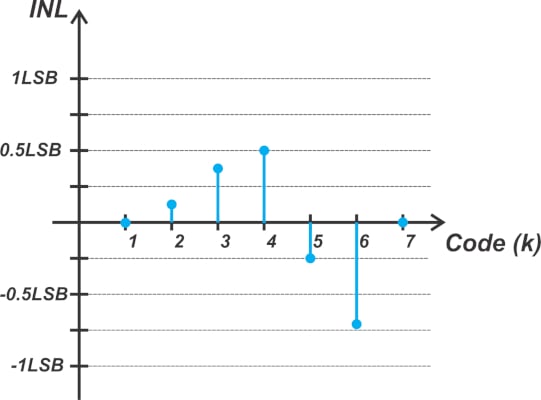
Figure 2. Example plot showing the INL against the code value.
INL is also commonly expressed as minimum and maximum values across all codes. The INL of our hypothetical ADC is between -0.71 LSB and +0.5 LSB. The INL plot not only represents the linearity performance of an ADC but also reveals some information about the internal architecture of the ADC. For example, sub-ranging ADCs have a triangular INL plot (Figure 3(a)), whereas flash ADCs typically have a random pattern (Figure 3(b)).
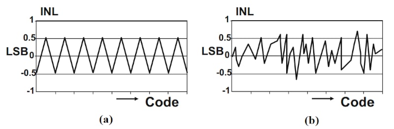
Figure 3. Example of a sub-ranging ADC triangular INL plot (a) and a flash ADC's random pattern plot (b). Image used courtesy of M. Pelgrom
INL: an Error Beyond the ADC Quantization Error
It’s important to note that the INL specifies an error in addition to the quantization error of the ADC. Since an ADC transforms the continuous analog input range to several discrete output codes, even an ideal ADC inherently introduces some error, known as the quantization error, into the system. If we apply a ramp input with a slope of 1 to an ADC, we can subtract the analog equivalent of the output code from the input to find the quantization error. This is illustrated in Figure 4.
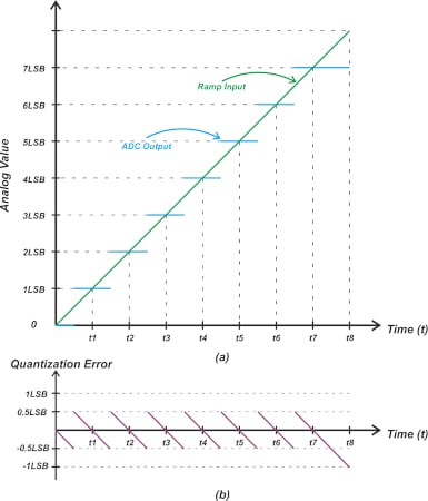
Figure 4. Example plots showing the quantization error.
In Figure 4, the green curve shows the ramp input, and the blue steps represent the analog equivalent of the codes produced by an ideal ADC. The lower diagram in Figure 4, however, shows the quantization error with a sawtooth shape. Let’s see how nonlinearity affects the error term. If we apply the ramp input to the non-ideal characteristic curve in Figure 1, we obtain the following error waveform (Figure 5).
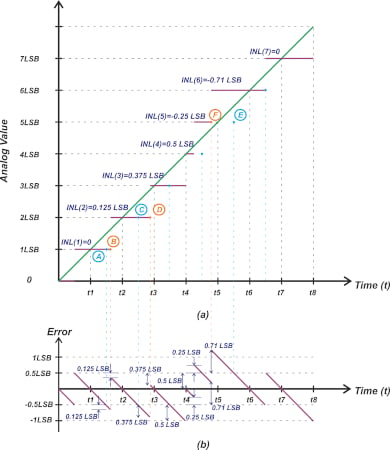
Figure 5. Example plots showing the analog equivalent of the ADC output code and ideal transform (a) and error waveform (b).
The purple steps in Figure 5(a) show the analog equivalent of the ADC output code, and the blue dots depict the ideal transition points of a uniform staircase response. As an example, consider the transition from code 1 to code 2. If this transition occurred at the ideal point (point A), the most negative error of code 1 would be -0.5 LSB. Since INL(2)=+0.125 LSB, the actual transition from code 1 to code 2 occurs at +0.125 LSB above the ideal value. Due to this delayed transition, the difference between the green curve and the ADC output becomes larger than 0.5 LSB at the transition point (point B). By examining the figure, you can confirm that the error at point B is given by:
\[Error_{B}=-0.5 \text{ } LSB-0.125 \text{ } LSB=-0.625 \text{ } LSB\]
Note that while this non-ideal effect extends the error of code 1 to -0.625 LSB, it reduces the upper limit of the error of the next code (code 2) to 0.5 LSB - 0.125 LSB = +0.375 LSB. You can see a similar change in the error waveform at point D that is caused by INL(3) = +0.375 LSB.
Let’s examine code 6 to see how a negative INL affects the error (INL(6 )= -0.71 LSB). In this case, the actual transition at (point F) occurs at 0.71 LSB below the ideal value (point E). Since the ADC output increments earlier than the expected value, a large positive error is produced. As shown in the error diagram, the error of code 6 can be as large as:
\[Error_{F}=0.5 \text{ } LSB+0.71 \text{ } LSB=+1.21 \text{ } LSB\]
With an ideal ADC, the quantization process produces an error of ±0.5 LSB. For a practical ADC, however, both the quantization process and INL contribute to the overall error of the system. In other words, the INL is an error beyond the quantization error.
The INL definition we have considered so far is perhaps the most useful and common definition of this specification. However, it should be noted that there are a few other definitions that are sometimes mentioned in textbooks and technical documents of ADC manufacturers. To avoid any confusion, we’ll take a look at other common definitions of INL in the rest of the article.
Redefining INL Code: Different Yet the Same Definition
Before we proceed with other definitions, it’s worthwhile to mention that one can view the definition used in Figure 1 in a slightly different way. Rather than defining INL as the deviation of code transitions from their ideal values, we can define it as the deviation of code transitions from a straight line that goes through the first and last code transitions. This is illustrated in Figure 6.
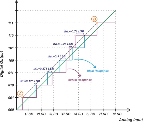
Figure 6. Plot showing the deviation of the code between actual response and ideal response.
In Figure 6, points A and B are the first and last transition points. Since we assume that the offset and gain errors are nullified before INL calculations, points A and B correspond to both the ideal and actual transfer functions. As you can see, the line that goes through points A and B also goes through all other transition points of the ideal characteristic (blue curve in the figure). Therefore, the deviation of an actual transition point from its corresponding ideal transition is equal to the deviation of that actual transition point from the straight line that goes through points A and B. Some references, such as the book “High-Speed Analog-to-Digital Conversion,” use this straight line to define the ADC INL. Also, note that this reference line is different from the linear model of the ADC (the green line in the figure) that was introduced in previous articles.
Defining INL—Code Center Line Definitions
For this type of definition, the ADC transfer characteristic is defined based on a straight line that goes through the ADC code centers. Figure 7 shows how one can define INL using a code center line.
Figure 7. Defining the INL using a code center line. Image used courtesy of R. Plassche
In the above example, the diagonal line is the line that goes through the midpoint of the steps of the ideal ADC (we’ve called this the linear model of ADC throughout the articles in this series). As illustrated in the diagram, the deviation of the midpoint of an actual step from the straight line is considered as the INL error of that code.
This example shows a shortcoming of this definition. As you can see, the adjacent transitions of code 1101 deviate from the ideal values. However, since the measured code center for 1101 coincides with the ideal value, the INL of this code is zero. With the definition used in Figure 1, the INL of code 1101 would be non-zero.
As a side note, the above image is taken from Rudy van de Plassche’s book. Rudy was a world- famous analog designer and inventor of many circuits and circuit ideas, such as chopper and stabilized amplifiers, that are widely used today.
Another code-center-based definition is shown in Figure 8.

Figure 8. Example plot showing the code center line definition. Image used courtesy of M. Demler
In this case, the reference line for calculating the INL error is the line that goes through the midpoint of the first and last steps of the actual transfer function. For a three-bit ADC, this is the line that goes through the midpoint of codes 001 and 110. The deviation of the midpoint of an actual step from this straight line is considered the INL error of that code.
In this particular example, the ADC transfer function has alternating wide and narrow codes in a way that the reference line obtained from the first and last codes intercepts the midpoint of all codes. As a result, the INL error is zero for all codes. This again highlights the shortcoming of the code center-based definition that cannot describe the nonlinearity of the transfer function in certain situations.
The INL definitions discussed in this article are categorized as endpoint-based definitions because they only use the first and last codes for deriving the reference line. Another method for defining the INL error is the best-fit method. In this case, a straight line fit through all codes is used as the reference line. The next article in this series will examine best-fit methods in detail.
Featured image used courtesy of Adobe Stock.
To see a complete list of my articles, please visit this page.


Thanks for sharing this knowledge ~