
Small-Signal MOSFET Models for Analog IC Design
The small-signal characteristics of MOSFETs play an important role in analog IC design. In this article, we learn how to model MOS transistors' small-signal behaviors.
As we explained in a previous article, MOSFETs are essential to modern analog IC design. However, that article primarily focused on the large-signal behavior of MOSFETs. Analog ICs normally use MOSFETS for small-signal amplification and filtering. In order to fully understand and analyze MOS circuits, we need to define the MOSFET’s small-signal behavior.
What is Small-Signal Analysis?
When we say “small-signal,” what exactly do we mean? To define this, let’s refer to Figure 1, which shows the output transfer characteristic of an inverter.
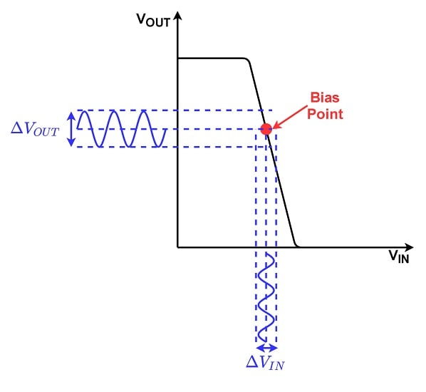
Figure 1. Transfer characteristic of an inverter.
Assume that:
- VIN and VOUT are both DC voltages.
- The value of VIN means we’re operating at the bias point (labeled in red).
In small-signal analysis, we apply a very small AC signal (ΔVIN), on top of the DC bias voltage. The resulting output AC voltage is amplified based on the slope (–AV) of the transfer characteristic at the bias point:
$$\Delta V_{OUT}~=~ -A_{V} \times \Delta V_{IN}$$
Equation 1.
Note that –AV is only negative due to the slope’s direction. We’ll return to AV later in the article. For now, the important takeaway is that the bias point (large-signal behavior) affects the amount of gain the output signal receives (small-signal behavior).
Small-Signal Parameters
Before we model our circuit’s behavior, we need to define our parameters. The main small-signal parameters of a MOSFET are:
- Transconductance (gm).
- Output resistance (ro).
- Intrinsic gain (AV).
- Body-effect transconductance (gmb).
- The unity gain frequency (fT).
Excepting fT, which we won’t discuss until we create our high-frequency MOSFET model, we’ll define and derive each of the above terms in the coming sections. We’ll start by looking at the I-V characteristic, transconductance.
Transconductance
As we already know, a MOSFET turns an input voltage into an output current. The ratio of the small-signal output current to the small-signal input voltage is known as the transconductance (gm). We can also think of transconductance as the derivative of the output current versus the gate-to-source voltage.
The transconductance can be defined for the linear region as:
$$\begin{array}{} g_{m,lin}~=~\frac{\delta I_{D}}{\delta V_{GS}}~=~\frac{\delta \left( \mu C_{ox} \frac{W}{L} \left[(V_{GS}~-~V_{th})V_{DS}~-~\frac{(V_{DS})^2}{2} \right] \right)}{\delta V_{GS}} \\~=~ \mu C_{ox} \frac{W}{L} V_{DS} \end{array}$$
Equation 2.
and for the saturation region, as:
$$\begin{array}{} g_{m,sat}~=~\frac{\delta I_{D}}{\delta V_{GS}}~=~ \frac{\delta \left[ \frac{1}{2} \mu C_{ox} \frac{W}{L} (V_{GS}~-~V_{th})^{2} \right]}{\delta V_{GS}} \\ ~=~ \mu C_{ox} \frac{W}{L} (V_{GS}~-~V_{th}) \end{array}$$
Equation 3.
where:
ID is the drain current
VGS is the gate-to-source voltage
VDS is the drain-to-source voltage
Vth is the threshold voltage
μ is the transistor mobility
Cox is the gate oxide capacitance
W is the width of the transistor
L is the length of the transistor.
These two equations lead us to a few interesting points:
- When in the linear region, the current gain of the transistor is dependent on the output voltage. It’s not at all dependent on the input signal. This isn’t ideal in practice, as the gain will change dramatically over the operation range.
- While in saturation, the transconductance is dependent only on the input voltage.
- Short, wide devices maximize the current gain for a given input bias voltage.
Output Resistance
The next parameter of interest is the output resistance (ro). This is defined as the change in the transistor’s drain-to-source voltage with respect to the drain current. We can find the output resistance by plotting the drain current versus VDS. The slope of the resulting line is equal to the inverse of ro.
Let’s take a look at the plot in Figure 2. We first saw this figure in a previous article about MOSFET structure and operation, where it helped us compare the drain currents of NMOS and PMOS transistors.

Figure 2. Drain current vs. VDS of an NMOS and a PMOS transistor. W / L = 10 μm / 2 μm.
A MOSFET has a small output resistance when in the linear region, and a large output resistance when in the saturation region. In the figure above, both the NMOS and PMOS transistor enter saturation at ~1.5 V.
Because—as we saw with the transconductance—the saturation region provides better small-signal performance, we’ll only concern ourselves with the output resistance when the transistor is in saturation. We can calculate this as:
$$\begin{array}{} &r_o ~=~\left( \frac{ \delta I_{D}}{ \delta V_{DS}} \right)^{-1} ~=~& \frac{1}{ \left( \frac{\delta I_{D}}{\delta V_{DS}}\right)} ~=~ \frac{1}{ \left( \frac{\delta \left[\frac{1}{2} \mu C_{ox} \frac{W}{L} \left(V_{GS}~-~V_{th} \right)^{2} \left(1~+~ \lambda V_{DS} \right) \right]}{\delta V_{DS}} \right) } \\ &~=~\frac{1}{\lambda I_{D}}~ \propto ~ \frac{L^{2}}{ \left( V_{D,sat} \right)^{2}}& \end{array}$$
Equation 4.
where λ is the channel-length modulation.
The relationship between ro and λ makes sense when you consider that the slope of the I-V curve in saturation results from channel-length modulation. Equation 4 also tells us that:
- ro decreases with drain current (ID).
- Because of the above, ro decreases with overdrive voltage (VD,sat).
- ro increases with transistor length (L).
Intrinsic Gain
Now that we know the output resistance and current gain of the transistor, we can calculate its maximum voltage gain. This is also known as the transistor’s intrinsic gain (AV). To better understand the concept of intrinsic gain, let’s examine the common-source amplifier configuration in Figure 3.

Figure 3. An NMOS transistor configured as a common-source amplifier.
Since an ideal current source has an infinite resistance, the small-signal output transfer function for this circuit can be calculated as:
$$\frac{\delta V_{OUT}}{\delta V_{IN}}~=~\frac{\delta V_{DS}}{\delta V_{GS}}~=~ g_{m} r_{o}~=~A_{V}$$
Equation 5.
From Equations 3 and 4, we can see that gm and ro are inversely related to the drain current. Using this knowledge, we can find an optimum value for the drain current that produces the largest gain possible for a single transistor—in other words, its intrinsic gain. For modern processes, the intrinsic gain is usually between 5 and 10.
Body-Effect Transconductance
The final small signal parameter we need to derive is the body-effect transconductance (gmb), which describes how the body effect influences the drain current. We can calculate this as:
$$g_{mb}~=~ \frac{\delta I_{D}}{\delta V_{BS}}~=~\frac{\delta I_{D}}{\delta {V_{TH}}} \frac{\delta V_{TH}}{ \delta V_{BS}}~=~g_{m} \eta$$
Equation 6.
where η is the back-gate transconductance parameter, and usually has a value between 0 and 3.
Low- and High-Frequency Models
Now that we’ve defined our parameters, we can build a circuit model that represents the small-signal operation of the transistor. Figure 4 depicts the small-signal behavior of a MOSFET at low frequencies.

Figure 4. MOSFET small-signal model.
At higher frequencies, we need to include the MOSFET’s parasitic capacitances (Figure 5).
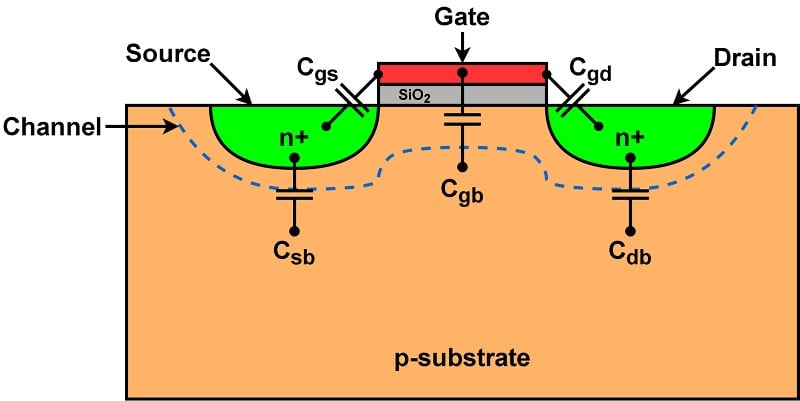
Figure 5. MOSFET structure with parasitic capacitances.
Represented above are:
- Cgs, the gate-to-source capacitance.
- Cgd, the gate-to-drain capacitance.
- Cgb, the gate-to-body capacitance.
- Csb, the source-to-body capacitance.
- Cdb, the drain-to-body capacitance.
The small-signal transistor model in Figure 6 includes all of these non-idealities except for the body capacitances.
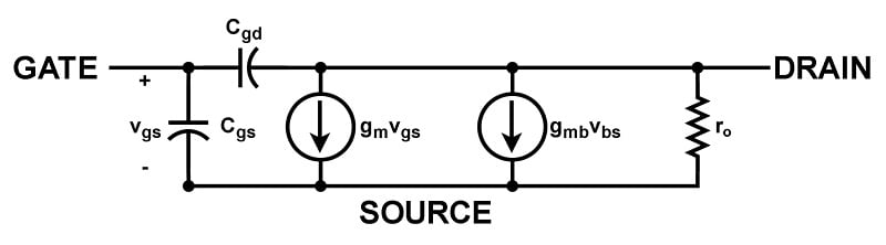
Figure 6. MOSFET small-signal model with capacitances.
From Figure 6, we can see that the intrinsic gain of the MOSFET in Figure 3 has a single-pole low-pass transfer function. We can now calculate the bandwidth of the transistor, which in this case would be the frequency at which the voltage gain is equal to 1 (0 dB). This is known as the unity gain frequency (fT).
To find fT, we short the output to ground and calculate the transconductance of Figure 6. Doing this gives us the following equation:
$$f_{T}~=~\frac{g_{m}}{C_{gs}~+~C_{gd}}~ \propto ~ \frac{V_{D,sat}}{L}$$
Equation 7.
From Equations 4 and 7, we see that to increase the gain, we would need to increase the length of the transistor. We also see, however, that this results in a lower bandwidth. The reverse is likewise true: decreasing the length of the transistor results in a higher bandwidth.
Looking Ahead
We now know how the MOSFET behaves with small-signal AC inputs, how to model this behavior, and how it relates to the large-signal behavior described in earlier articles. With these tools in hand, we’re ready to build and analyze analog circuits with MOSFETs!
Featured image used courtesy of Adobe Stock; all other images used courtesy of Nicholas St. John


definition of ro in Equation 4 is wrong. ro is the derivative of Id with respect to Vds.