Simulating the Short-Circuit Power Dissipation of a CMOS Inverter
Current briefly flows through both transistors during logic-level transitions. This article explores the resulting power dissipation and provides some helpful LTspice tips for measuring current and power.
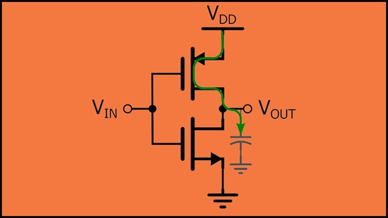
In the first article of this series, we examined dynamic and static power dissipation in a CMOS inverter. In a subsequent article, we used LTspice simulations to gain additional insight into power consumption caused by capacitive charging and discharging. As part of that discussion, we created the LTspice inverter circuit shown in Figure 1.

Figure 1. An LTspice schematic of a CMOS inverter with load resistance and capacitance.
We’ll continue using the above schematic in this article, which investigates “short-circuit” or “shoot-through” current. These two terms refer to the current that flows through both the NMOS and the PMOS transistors in Figure 1 during the output transition periods.
The short-circuit current flow is possible because as the input voltage—the gate voltage controlling the two transistors—changes, the inverter passes through an electrical region in which both the NMOS channel and the PMOS channel are conductive.
Measuring Short-Circuit Current
We want to measure only the current that flows from VDD to ground as a result of shoot-through. This means that we must exclude the current that charges and discharges the load capacitor, C1, during the transitions.
Short-Circuit Current During a Rising Output Transition
In Figure 2, we’ve magnified the center portion of the inverter circuit. The probe location for the low-to-high output transition is shown by the green dot at the drain of the NMOS transistor (M1).

Figure 2. The green dot indicates where we measure shoot-through current as the output changes from logic-low to logic-high.
During a low–to-high output transition, charging current flows:
- From VDD.
- Through the PMOS transistor (M2).
- To the load capacitor (C1).
Meanwhile, short-circuit current flows:
- From VDD.
- Through the PMOS transistor.
- Through the NMOS transistor.
- To ground.
By probing the wire segment marked by the green dot in Figure 2, we measure the current flowing through the two transistors after the charging current has veered off toward the capacitor. The simulation results are shown in Figure 3.

Figure 3. Inverter shoot-through current during a rising output transition.
The measured current peaks when the input is at 0.9 V. At this voltage, both the NMOS and PMOS transistors are weakly on. This allows current to flow directly from VDD to ground.
Short-Circuit Current During a Falling Output Transition
For the high-to-low output transition, the situation is reversed. Discharging current flows:
- From the load capacitor.
- Through the NMOS transistor (M1)
- To ground.
The short-circuit current’s path, however, remains unchanged. It still passes through M2 and then M1 on its way to ground. Thus, we probe the current at the drain of the PMOS transistor, before the node at which discharge current arrives from the capacitor. The probe location is marked in Figure 4.

Figure 4. The green dot indicates where we measure shoot-through current as the output changes from logic-high to logic-low.
Figure 5 shows the LTspice simulation results for the falling output transition.

Figure 5. Inverter shoot-through current during a falling output transition.
Again, the current peaks when the input voltage is near its midpoint at 0.9 V. This short-circuit current causes power dissipation as it flows through the NMOS and PMOS resistance.
Measuring Instantaneous Power Dissipation
Two things prevent us from easily converting our transistor current measurements into numerical estimates of power dissipation:
- The current isn’t flowing through a fixed resistance, so we can’t directly apply P = I2R.
- The transistors’ drain-to-source voltages aren’t constant, so we can’t directly apply P = IV.
LTspice, however, is not at all opposed to performing the necessary calculations. If you press the Alt key (Cmd on a Mac) while clicking on a component, LTspice will plot the instantaneous power dissipation for that component. Let’s try this out.
The Rising Output Transition
The red trace in Figure 6 plots the power consumed by the NMOS during a low-to-high output transition. Because no charging or discharging current flows through the NMOS during a rising transition, this power dissipation results primarily from the short-circuit current.

Figure 6. Instantaneous NMOS power dissipation during a low-to-high output transition.
By contrast, Figure 7 shows the instantaneous power dissipation for the PMOS over the same transition. Because charging current does flow through this transistor, its power consumption is significantly higher.

Figure 7. Instantaneous PMOS power dissipation during a low-to-high output transition.
The Falling Transition
For a high-to-low output transition, the capacitance current flows through the NMOS rather than the PMOS. The power dissipation of the NMOS (Figure 8) is now greater than that of the PMOS (Figure 9).

Figure 8. Instantaneous power dissipation of the NMOS during a high-to-low output transition.

Figure 9. Instantaneous power dissipation for the PMOS during a high-to-low output transition.
For a falling transition, the PMOS is the component we want to examine to find the inverter’s short-circuit power dissipation.
How Does LTspice Get These Results?
LTspice doesn’t just calculate the power—it also lets us know, via the trace labels, exactly how it performs its calculations. For example, we can see that the power dissipation for the NMOS (M1) during a rising transition is equal to:
$$P_{M1}~=~(V_{OUT}~\times~I_{d(M1)})~+~(V_{IN}~\times~I_{g(M1)})$$
where Id is the transistor’s drain current (short-circuit current) and Ig is the gate current.
The power dissipation for the PMOS (M2) during the same transition is:
$$P_{M2}~=~(V_{(V_{OUT,V_{+}})}~\times~I_{d(M2)})~+~(V_{(V_{IN},V_{+})}~\times~I_{g(M2)})$$
where V+ refers to the supply voltage (VDD in our original schematic).
In this particular case, the power dissipation is almost entirely due to the drain current. However, the presence of Ig in both equations should serve as a reminder that gate current can also contribute to total power consumption.
Energy Loss and Average Power Dissipation
Ultimately, the concepts and simulations in this article series are meant to provide a toolkit for analyzing dynamic power dissipation in a CMOS inverter. In that spirit, I’d like to present one more piece of LTspice functionality before we finish up. While it won’t help us find out anything else about short-circuit power, it’s entirely relevant to the broader topic of dynamic power dissipation.
If we hold Ctrl and click on the trace label for one of our instantaneous power waveforms, LTspice will open a cursor box. The bottom field in this box, labeled “Integral,” reports the amount of energy lost over the course of the simulated transition. For example, Figure 10 shows the total energy loss for the NMOS during a low-to-high output transition.

Figure 10. Energy lost through the NMOS transistor over the course of one rising transition.
Figure 11 shows the total NMOS energy loss for a falling transition.

Figure 11. Energy lost through the NMOS during one falling transition.
Once we’ve found the total energy loss of the PMOS (Figures 12 and 13) as well, we can estimate the average dynamic power dissipation for our inverter.

Figure 12. Energy lost through the PMOS during one rising transition.

Figure 13. Energy lost through the PMOS during one falling transition.
For ease of reference, the energy loss values are reproduced in Table 1. Note the “Total” column on the right—we’ll be using those numbers in a moment.
Table 1. Total energy loss of the transistors during one rising and one falling transition.
| NMOS | PMOS | Total (NMOS + PMOS) | |
| Rising | 3.563 pJ | 12.631 pJ | 16.194 pJ |
| Falling | 15.616 pJ | 1.784 pJ | 17.400 pJ |
We can now estimate the inverter’s average dynamic power dissipation as follows:
$$P_{Average}~=~(P_{Rising}~+~P_{Falling})~\times~f$$
where f is the number of cycles per second.
For this simulation, we have PRising = 16.2 pJ and PFalling = 17.4 pJ. Let’s say the inverter is switching at 500 Hz. Recalling that one watt equals one joule per second (1 W = 1 J/s), this gives us an estimated power dissipation of:
$$P_{Average}~=~(16.2~\text{pJ}~+~17.4~\text{pJ})~\times~500~\text{Hz}~=~16.8~\text{nW}$$
With that, you’re ready to experiment with techniques for reducing dynamic current flow and power dissipation in a CMOS inverter. This concludes my series on CMOS inverter power dissipation, though we may return to these simulations in the future. In the meantime, I hope you’ve found our discussions helpful.
All images used courtesy of Robert Keim