
Power Dissipation of a CMOS Inverter
This article explains dynamic and static power consumption in a CMOS inverter circuit.
The development of the CMOS inverter, which provides essential functionality for integrated circuits, was a turning point in the history of technology. This logic circuit highlights the electrical properties that make CMOS so uniquely suitable for high-density, high-performance digital systems.
One advantage of CMOS is its efficiency. CMOS logic requires current flow only when changing states—a CMOS circuit that’s simply maintaining a logic-high or logic-low voltage dissipates very little power. Low power dissipation is a desirable feature in general, and it’s particularly beneficial when you’re trying to pack as much transistor functionality as possible into a small space.
As computer CPU fans remind us, adequately removing heat from an integrated circuit can be difficult. It would be far more difficult without the CMOS inverter and other, similar CMOS circuits. In this article, the first in a three-part series, we’ll review key characteristics of the CMOS inverter and discuss its two primary types of power dissipation: dynamic and static. We'll delve more deeply into dynamic power dissipation in the next two articles.
Structure and Operation of a CMOS Inverter
A CMOS inverter is composed of an NMOS transistor and a PMOS transistor connected together. Figure 1 shows the schematic for a basic CMOS inverter.
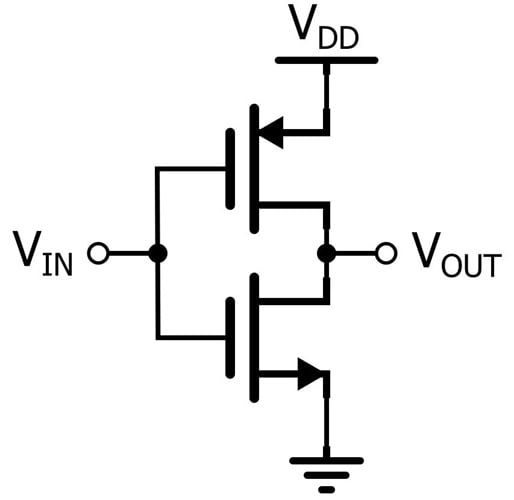
Figure 1. A CMOS digital inverter uses one NMOS and one PMOS transistor.
The basic operation of a CMOS inverter is quite straightforward:
- When the input terminal is driven to the logic-high voltage, the upper PMOS transistor blocks current and the lower NMOS transistor conducts current. The output terminal is thus connected to 0 V through a low-resistance path.
- When the input terminal is driven to the logic-low voltage, the PMOS conducts and the NMOS blocks. The output is connected through a low-resistance path to VDD.
In this way, a logic-high input creates a logic-low output, and a logic-low input creates a logic-high output.
Dynamic Power Consumption
Power is consumed whenever current is flowing through a conductive element. We see this relationship in the basic formula for electric power:
$$P~=~I~\times~V$$
Equation 1.
Though a CMOS inverter doesn’t require current flow in its steady state, power is consumed during its logic transitions. This dynamic power loss comes in two types:
- Switching power dissipation.
- Short-circuit power dissipation.
Let’s take a look at each.
Switching Power Dissipation
When an input logic transition occurs, transient current must flow in order to charge or discharge capacitance in the circuit. During a low-to-high output transition, current flows to charge up the load capacitance as the output voltage increases to VDD. Figure 2 shows the path taken by this current.
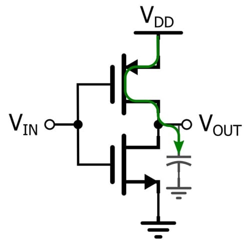
Figure 2. The flow of charging current during a low-to-high output transition.
Current also flows during a high-to-low output transition (Figure 3), discharging capacitance as the output voltage decreases to ground potential.
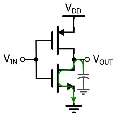
Figure 3. The flow of discharge current during a high-to-low output transition.
To estimate the switching loss of a CMOS inverter, we use the following equation:
$$P_{switching}~=~C_{L}~\times~V_{DD}^{~~~~~2}~\times~f$$
Equation 2.
where:
CL is the expected load capacitance
f is the switching frequency.
CL × VDD2 calculates the amount of energy required for one switching cycle. To convert this result from energy to power, we multiply it by the number of cycles per second (f), giving us the equation above.
Short-Circuit Power Dissipation
Another type of dynamic power dissipation is caused by short-circuit current. Also known as shoot-through current, this is a transient condition that occurs during an inverter’s logic level transitions.
When a CMOS inverter is settled in a logic state, one of its two transistors is in a non-conductive mode. Consequently, current can’t easily flow from VDD to ground. When the inverter changes states, however, there’s a brief crossover period during which both the NMOS and the PMOS have some degree of conductivity. Energy is lost as current flows through the resulting short circuit (Figure 4).
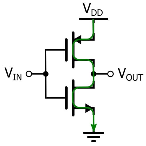
Figure 4. The NMOS and PMOS transistors briefly create a short circuit during logic-level transitions, allowing current to flow from VDD to ground.
Static Power Consumption
Throughout this article, I’ve avoided saying anything along the lines of “absolutely no steady-state power dissipation occurs in a CMOS inverter.” The fact is that field-effect transistors aren’t ideal switches. Even in the OFF state, leakage currents can flow from the drain to the source and from the drain or source to the substrate.
If the magnitude of these leakage currents is known, the resulting power dissipation can be calculated using the formula:
$$P_{static}~=~I_{leakage}~\times~V_{DD}$$
Equation 3.
Dynamic power consumption used to be much higher than static power consumption. Nowadays, static power can be significant. As CMOS feature sizes decrease, its contribution to total dissipation approaches that of dynamic power.
Finally, note that static power is a function of operating temperature. As temperature increases, static power dissipation also increases.
Wrapping Up
The CMOS inverter is useful both as a standalone logic operation and as a component of higher-order logic operations. CMOS inverters are also used to create buffers at the outputs of digital circuits with low drive capability. The inverters provide analog amplification to reduce the rise and fall times of a signal. They can also restore a signal to full logic levels.
In this article, we briefly discussed the operation of a CMOS inverter and examined the dynamic and static power dissipation of this foundational logic circuit. In the next two articles of this series, we’ll use LTspice simulations to explore the topic of dynamic power dissipation in greater detail.
All images used courtesy of Robert Keim


