Offset and Gain Calibration Functions in Precision ADCs: Self-calibration
Learn about the self-calibration or internal calibration function in an analog-to-digital converter (ADC).
Previously in this series, we discussed that a two-point calibration can be used to remove the offset and gain errors of an ADC (analog-to-digital converter). Depending on the hardware employed, you might use either a fixed-point or floating-point method to implement the calibration equations. An alternative approach is to use ADCs that include integrated calibration functions since there are different types of calibration functions that might be found in a precision ADC, namely:
- Self-calibration
- System calibration
- Background calibration
In this article, we’ll explore the self-calibration function.
Options for ADC Calibration
Some ADCs support calibration modes which can simplify design and help us save some central processing unit (CPU) cycles from the system processor. In this case, you only need to adjust the ADC settings, send the appropriate calibration command, and wait for the ADC to determine the offset and gain errors.
The ADC then stores the calibration information in its on-chip registers and uses it to correct the subsequent readings for offset and gain errors. Figure 1 shows an example calibration block diagram of the ADS1246 from Texas Instruments (TI).
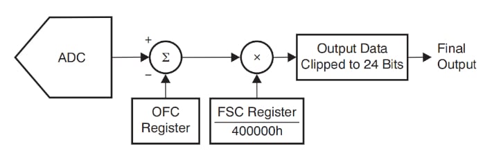
Figure 1. Example ADS1246 block diagram showing a calibration block. Image used courtesy of TI
In Figure 1, the offset register (OFC) and full-scale register (FSC) contain the appropriate calibration values. The value of the OFC is subtracted from the digital value produced by the A/D (analog-to-digital) conversion process, and the result is multiplied by FSC divided by 400000h.
For example, with FSC = 800000h, the A/D conversion result will be multiplied by 2 because the FSC value is normalized to 1.0 at code 400000h. The calibration function of the ADS1246 can be described by the following equation:
\[Final\,Output\,Code=(Input-OFC)\times\frac{FSC}{400000h}\]
After calibration is initiated, the ADC automatically sets the value of the OFC and FSC registers. However, with the ADS1246, it is possible for the user to directly write some values to these registers, which enables the user to have more control over the calibration function.
Note that while most ADCs first subtract the offset calibration coefficient and then multiply it by the gain error coefficient, there are ADCs that first adjust the slope of the transfer function and then correct for the offset error. For example, the ADCs incorporated in the MPC5500 family from NXP use a multiply-accumulate unit to implement the calibration function (Figure 2).
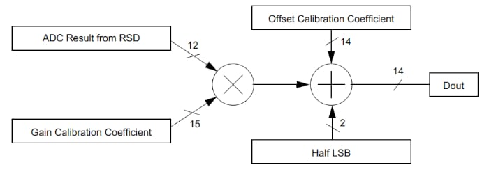
Figure 2. Example MPC5500 family block diagram. Image used courtesy of NXP
Obviously, for a given system, the two methods depicted in Figures 1 and 2 will have different gain and offset calibration coefficients.
In general, a calibration procedure effectively consists of one or two ADC conversions performed on known input voltages. The ADC uses the results of these conversions to determine the offset and slope of the input-output characteristic curve and updates its calibration registers accordingly.
Analog-to-digital Converter Self-calibration or Internal Calibration
Self-calibration, sometimes called internal calibration, attempts to characterize and compensate for the offset and gain errors of the internal blocks of the ADC. For example, with a delta-sigma (ΔΣ) ADC that has an integrated PGA (programmable gain amplifier), a self-calibration removes the DC errors from both the PGA and the ΔΣ modulator. With some ADCs, such as the AD7124-4, the self-calibration function can perform both offset (zero-scale) and gain (full-scale) calibrations. However, with some other ADCs, such as the AD7172-2, the self-calibration procedure only performs offset calibration.
ADC Internal Offset Calibration
For internal offset calibration, the inputs of the selected ADC channel are internally shorted. In addition, the output code is compared with the ideal value to determine the offset error. With most ADCs, such as the ADS1260-Q1, an input multiplexer is incorporated to disconnect the inputs from the outside world and internally connect them to a common voltage to perform offset calibration. The input multiplexer of the ADS131M06, which is relatively simpler than that of the ADS1260-Q1, is shown in Figure 3.
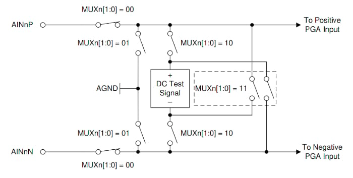
Figure 3. Diagram showing the input multiplexer for ADS131M06. Image used courtesy of TI
As you can see, one of the multiplexer configurations, MUXn[1:0] = 01, shorts both inputs to the ground. This multiplexer configuration can be used for offset calibration. On the other hand, some ADCs only disconnect one of the inputs from the external circuitry. As an example, consider the internal connection of the AD7124-4, which is depicted in Figure 4.
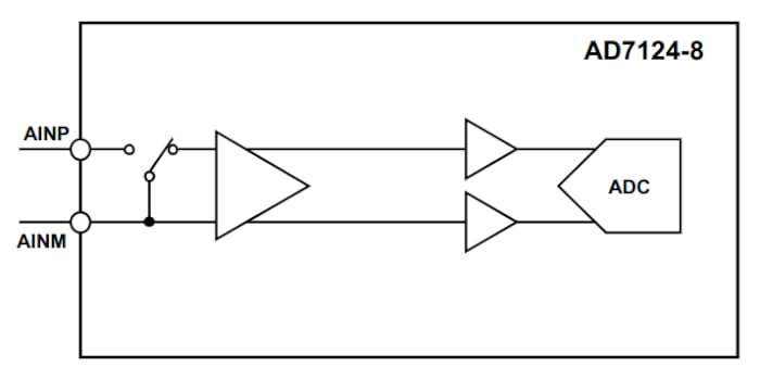
Figure 4. Block diagram showing the internal connection of the AD7124-4. Image used courtesy of Analog Devices
During offset calibration, both inputs are shorted together. However, the negative input remains connected to the external circuitry. That’s why the device datasheet recommends that designers ensure that any excess noise and interference are not present at the negative input during offset calibration. Also, the voltage of this input is not allowed to exceed the rated limit when calibration is being performed.
ADC Internal Full-scale Calibration
The full-scale calibration is normally performed by applying an internally-generated full-scale voltage to the ADC inputs. If the ADC has an input range of ±VREF, the inputs are internally tied to the +VREF and -VREF lines. Knowing that the inputs are at the full-scale level, the ADC can determine the required gain calibration coefficients. If the ADC has an integrated PGA, the internally generated voltage is normally the reference voltage of the ADC divided by the selected gain of the PGA to avoid overranging the ADC. This allows the device to support internal full-scale calibration at each gain setting.
ADCs with calibration functions normally repeat zero-scale and full-scale measurements a certain number of times (e.g. 16 times) and average the conversion results to compute the calibration values. Averaging the data reduces the conversion noise and improves the calibration accuracy.
Effectiveness of ADC Self-calibration
Below, Table 1, is an excerpt from the AD7124-4 datasheet.
Table 1. Data used courtesy of Analog Devices
|
Parameter1 |
Min |
Typ |
Max |
Unit |
Test Conditions/Comments |
|---|---|---|---|---|---|
|
ADC |
|
|
|
|
|
|
Offset Error5 |
|
|
|
|
|
|
Before Calibration |
|
±15 |
|
μV |
Gain = 1 to 8 |
|
|
|
200/gain |
|
μV |
Gain = 16 to 128 |
|
After Internal Calibration / System Calibration |
|
In order of noise |
|
|
|
|
Gain Error5,7 |
|
|
|
|
|
|
Before Internal Calibration |
-0.0025 |
|
+0.0025 |
% |
Gain = 1, TA = 25°C |
|
|
|
-0.3 |
|
% |
Gain > 1 |
|
After Internal Calibration |
-0.016 |
+0.004 |
+0.016 |
% |
Gain = 2 to 8, TA = 25°C |
|
|
|
±0.025 |
|
% |
Gain = 16 to 128 |
|
After System Calibration |
|
In order of noise |
|
|
|
Before applying offset calibration, the ADC offset is ±15 μV. However, after the offset calibration, the offset error is in the order of the noise, which is less than 400 nV RMS according to the device datasheet. Similarly, the gain calibration significantly reduces the gain error of the ADC.
Figure 5 compares the error of an RTD measurement system with and without ADC calibration. The ADC used in this example is AD7124-8.
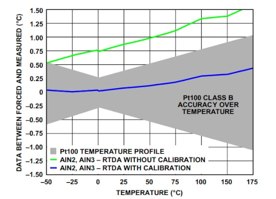
Figure 5. Example RTD measurement system using AD7124-8. Image used courtesy of Analog Devices
Without calibration, the measurement error is outside the expected profile of the Pt100 RTD. However, a one-time calibration of the ADC offset and gain errors at 25 °C leads to an error well within the expected range. Note that, in this example, the offset and gain errors produced by the external circuit components are not removed. For a comprehensive examination of the calibration effect on common RTD configurations, please refer to this reference design from Analog Devices.
As the results from Figure 5 and the above ADI reference design suggest, many applications should meet the design goals by simply removing the ADC offset and gain errors. However, with more demanding applications, we might need system calibration to remove the offset and gain errors from both the ADC and the external circuitry.
Let’s take a quick look at an RTD application example to learn how significant the errors from external circuitry can be.
Calculating ADC Errors—How Effective is System Calibration?
Consider the 3-wire, ratiometric RTD measurement system in Figure 6.
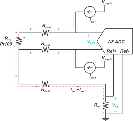
Figure 6. Example 3-wire ratiometric RTD measurement system.
Assume that the excitation currents (Iexc1 and Iexc2) are 0.5 mA and the reference resistor is RREF = 1.6 kΩ, yielding a reference voltage of 1.6 V. Major error sources in this circuit are:
- ADC offset and gain errors
- ADC integral nonlinearity (INL)
- Tolerance of the reference resistor
- Matching between Iexc1 and Iexc2
Assume that the excitation currents are perfectly matched or the current swapping technique is used; thus, the current mismatch error is negligible. This leaves us with one major external error source: Rref tolerance.
Let’s see how significant this error can be. With the above ratiometric circuit, the digital output produced by an n-bit ADC can be typically described by the following equation:
\[Digital\,Value\,=\frac{Analog\,Input\,Voltage}{ADC\,Reference\,Voltage}\times(2^{n}-1)\]
Assuming Iexc1 = Iexc2, the above equation simplifies to Equation 1:
\[Digital\,Value\,=\frac{R_{rtd}}{2R_{ref}}\times(2^{n}-1)\]
Equation 1.
Suppose that the actual value of Rref is slightly different from its ideal value and is given by:
\[R_{ref,m}=R_{ref}(1+\alpha)\]
Where α is a small value. By substituting Rref, m in Equation 1, it yields:
\[Digital\,Value=\frac{R_{rtd}}{2R_{ref}(1+\alpha)}\times(2^{n}-1)\]
Using the Taylor series concept, we can approximate $$\frac{1}{1+ \alpha}$$ with 1- α. Therefore, we obtain:
\[Digital\,Value=\frac{R_{rtd}}{2R_{ref}}\times(2^{n}-1)(1-\alpha)\]
Comparing this with the ideal relationship in Equation 1, we observe that a small error in Rref leads to an identical error in the slope of the transfer function. If we use a 0.1% reference resistor (α = 0.001), the actual gain of the system will be 0.1% different from its ideal value, meaning that we have a gain error of 0.1% due to the Rref tolerance. This gain error can be comparable with the ADC gain error, depending on the ADC you choose.
For example, without calibration, the ADS1260-Q1 has a maximum gain error of 0.6%. Therefore, in a demanding application, a system calibration can significantly improve accuracy. To learn more about the error sources in RTD applications, please refer to this reference design from TI. In the next article, we’ll continue this discussion and explore system calibration and background calibration modes in precision ADCs.
Featured image used courtesy of Wikipedia
To see a complete list of my articles, please visit this page.