
MOSFET Structure and Operation for Analog IC Design
Learn about the theory and implementation of MOSFETs, a key component of today’s analog integrated circuits.
Transistors—devices that translate an input voltage to an output current, or vice versa—are what make analog integrated circuit (IC) design possible. Today, analog ICs primarily use metal-oxide semiconductor field effect transistors, better known as MOS transistors or MOSFETs. In this article, we’ll introduce the physical implementation of MOSFETs and their theory of operation.
The MOSFET structure
An MOS transistor is a four-terminal device consisting of a gate (G), drain (D), source (S), and body (B). Figure 1 illustrates the two types of MOS transistor: the N-channel MOSFET (NMOS) and the P-channel MOSFET (PMOS). Generally speaking, these two channel types behave as the inverse of one another.

Figure 1. NMOS and PMOS schematic symbols. Image used courtesy of Nicholas St. John
The input voltage is connected to the gate terminal. The voltage level determines the drain current, which is the current that flows from the drain to the source terminals. In an NMOS transistor, the drain is normally at a higher voltage than the source; the opposite is true for a PMOS.
Lastly, we have the body terminal, which connects to the substrate that the transistor is built on. The body terminal for the NMOS transistor is tied to the lowest possible voltage in the circuit (ground in a single-supply system) whereas the PMOS body terminal is connected to the highest voltage level (VDD of the circuit).
In digital circuits, the source and body terminals are typically tied together. For this reason, you may see schematics that show the MOSFET as a three-terminal device with only the gate, source, and drain.
Figure 2 compares the basic physical structure of an NMOS transistor, on the left, with that of a PMOS transistor, on the right. Both transistors are built on top of a lightly P-doped silicon substrate. This is true of any transistor within an integrated circuit.

Figure 2. Physical structure of NMOS and PMOS transistors. Image used courtesy of UT Dallas
An insulator (normally silicon dioxide) is placed on top of the silicon substrate, and a gate terminal made of either polysilicon or metal is placed on top of the insulator. This is meant to prevent leakage from the gate terminal to the source, drain, and/or body terminals.
For the NMOS, the source and drain terminals are implemented by creating highly N-doped areas within the substrate. Note that there’s no physical difference between the source and drain terminals, making them interchangeable. This brings us to the body terminal. So as to provide a good electrical connection, it’s heavily doped with the same polarity as the substrate.
The PMOS device has the same structure as the NMOS, but with opposite dopant polarities. The PMOS body is a lightly N-doped region within the total P-type substrate, forming what’s referred to as an N-well.
The width (W) and length (L) of a transistor affect its other characteristics. This can be hard to see in two-dimensional diagrams, so I’ve included one that shows a three-dimensional view (Figure 3).
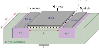
Figure 3. Three-dimensional NMOS transistor structure. Image used courtesy of Nicholas St. John
MOSFET Operating Regions
Now that we’ve examined the basic structure of the MOSFET, let’s dive into the theory of operation.
Cutoff Region
The electrical behavior of the MOSFET is determined by the voltage levels at each of its four terminals. For the NMOS in Figure 4, the gate and drain terminals are connected to independent voltage sources. The source and body are connected to ground.
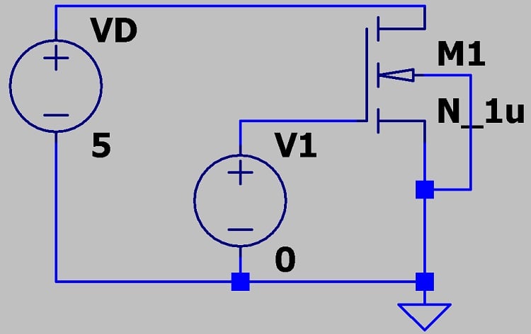
Figure 4. NMOS transistor with voltage sources applied. Image used courtesy of Nicholas St. John
Because the NMOS is an N-channel device, it only conducts current if a channel of electrons is formed between the source and drain (hence their negative doping). There’s no channel between the source and drain when the gate is at 0 V, so no current flows. This is known as the cutoff region.
As the gate voltage (VGS) increases, electrons are attracted to the area underneath the gate. Eventually, the gate voltage becomes positive enough for a channel to form, and a current begins to conduct from the drain to the source. The voltage at which this occurs is known as the threshold voltage (Vth). Figure 5 shows the threshold at which the drain current begins to increase, along with the exponential I-V curve that follows.
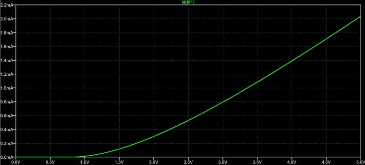
Figure 5. Drain current (y-axis) vs. gate voltage (x-axis) of NMOS from Figure 3. Image used courtesy of Nicholas St. John
VGS must be greater than Vth for the transistor to conduct current. When VGS is less than Vth, the transistor is in cutoff.
A PMOS transistor operates the same way, except that the source and body are tied to the maximum supply voltage (Figure 6).
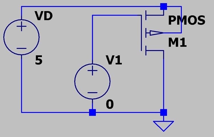
Figure 6. PMOS with voltage sources applied. Image used courtesy of Nicholas St. John
The threshold voltage of a PMOS transistor is negative. This means that the gate voltage must be less than the source voltage by at least the threshold voltage before the transistor begins to conduct. Figure 7 plots gate voltage and drain current for the PMOS in Figure 6.
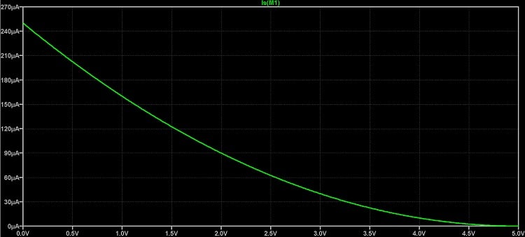
Figure 7. Drain current (y-axis) vs. gate voltage (x-axis) for a PMOS transistor. Image used courtesy of Nicholas St. John
As we can see, the PMOS conducts more current when |VGS| becomes larger than |Vth|.
Linear Region
Now that we’ve covered VGS, it’s time to look at how the drain-to-source voltage (VDS) affects the transistor’s electrical behavior.
Let’s assume that we’re looking at an NMOS where VGS > Vth, meaning that there is a channel of electrons between the drain and source. If VDS is greater than 0, current begins to flow. The drain current will increase in proportion to VDS, and the transistor is said to be operating in the linear region. Other common names for this region include triode, ohmic, and active.
We can calculate the drain current (ID) for an NMOS transistor via the following equation:
$$I_{D}~=~\mu C_{ox} \frac{W}{L} \left[(V_{GS}~-~V_{th} ) V_{DS}~-~ \frac{(V_{DS})^{2} }{2} \right]$$
Equation 1.
where:
µ is the mobility of the minority carrier within the substrate
Cox is the oxide capacitance from the gate oxide
\(\frac{W}{L}\) is the width-to-length ratio of the transistor.
For the PMOS, the equation is almost the same, but the voltage references are flipped and µ now refers to holes rather than electrons:
$$I_{D}~=~\mu C_{ox} \frac{W}{L} \left[(V_{SG}~-~V_{th} ) V_{SD}~-~ \frac{(V_{SD})^{2}}{2} \right]$$
Equation 2.
Both of the equations above are taken from “CMOS Circuit Design, Layout, and Simulation” by Dr. Jacob Baker.
Saturation Region
If the drain voltage continues to increase, eventually we reach a point where the drain terminal begins to pinch off, as illustrated in Figure 8. When this happens, the drain current will no longer increase as rapidly as it did before—in fact, it loses all connection to VDS. This is when the transistor enters the saturation region, where MOSFETs in analog ICs commonly operate.
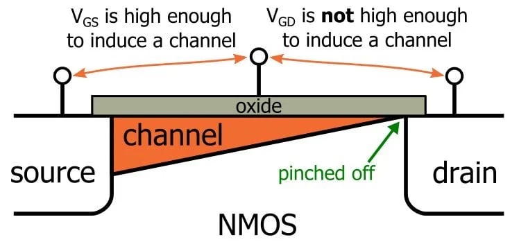
Figure 8. Pinch-off in transistors. Image used courtesy of All About Circuits
Pinch-off occurs when \(V_{DS}~=~V_{GS}~-~V_{th}\). This value is referred to as the overdrive voltage (Vov).
In theory, a transistor in saturation has an infinite impedance, making it an excellent current source. It also has a high voltage-to-current gain, or transconductance.
The drain current in saturation can be found using the square-law equation:
$$I_{D}~=~\mu C_{ox} \frac{W}{L} (V_{GS}~-~V_{th} )^{2}$$
Equation 3.
We can see from this equation that the drain current is independent of the drain voltage once the transistor goes into saturation. Having only VGS and the transistor dimensions to tweak reduces variation and simplifies design. In the real world, transistor non-idealities mean that the drain voltage still has some effect on the drain current.
Figure 9 shows transistor drain current versus the VDS (or VSD) for both NMOS and PMOS transistors. The transfer into the saturation region occurs at ~1.5 V. Note that neither drain current curve has zero slope at this point.
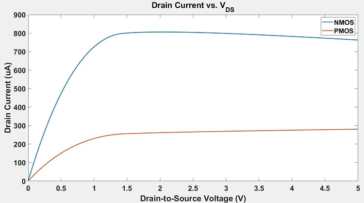
Figure 9. Drain current vs. VDS of NMOS and PMOS transistors. (W / L) = 10 µm / 2 µm. Image used courtesy of Nicholas St. John
The NMOS transistor current is much larger than that of the PMOS, even when the overdrive voltages and transistor dimensions are the same. This is because the mobility of holes in silicon is much slower than that of electrons—450 cm2/V·s for the former, compared to ~1300 cm2/V·s for the latter. The result is a far lower PMOS drain current. For this reason, many complementary MOSFET (CMOS) designs use PMOS transistors with width-to-length ratios two to three times larger than those of the NMOS transistors.
Up Next
MOSFETs are highly versatile devices—they can act as voltage-controlled switches, resistors, or amplifiers, depending on which region they’re operating in. In this article, we discussed the main operating regions and basic physical structures of MOS transistors. Next time, we’ll examine their non-idealities.


Nice introduction to MOSFET. Just to point in Figure 9 that shows transistor drain current versus VDS, it should have a positive slope for NMOS.