MOSFET Non-Idealities in Analog IC Design
MOS transistors exhibit a wide variety of second-order effects not covered by ideal models. To design analog integrated circuits that will work in the real world, we need to understand these non-idealities.
In the previous article, we introduced the basic MOSFET structure and operating regions. The models we discussed depicted an ideal MOSFET, and were fairly accurate for early MOS transistors due to their long channel sizes. However, subsequent research and the continued miniaturization of transistors have both revealed a slew of non-idealities in transistor behavior. This article will go over the basics of these non-idealities and how they affect transistor performance in analog integrated circuits.
Parasitic Capacitances
Due to the physical implementation of the MOSFET, the following parasitic capacitances are formed between terminal junctions:
- CGS: gate-to-source capacitance.
- CGD: gate-to-drain capacitance.
- CGB: gate-to-body capacitance.
- CSB: source-to-body capacitance.
- CDB: drain-to-body capacitance.
When designing analog ICs that include MOSFETs, these capacitances play a large role in circuit bandwidth. Figure 1 illustrates their locations.
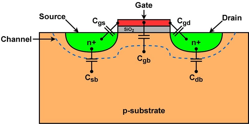
Figure 1. MOSFET structure with parasitic capacitances.
The capacitance values change with respect to the operating region, as we’ll discuss in the coming sections.
Gate-to-Source and Gate-to-Drain Capacitances
While this isn’t shown in Figure 1, the source and drain extend slightly under the gate during transistor fabrication. In the area where the gate overlaps either the source or the drain, a capacitor forms with the gate oxide (SiO2) as the dielectric between them. The length of this overlap is called Ldiff.
The value of the gate-to-source (or drain) capacitor formed by the oxide capacitance (Cox) can be calculated as:
$$C_{GS}~=~C'_{ox}~\times~W~\times~L_{diff}$$
Equation 1.
where:
C’ox is equal to \(\frac{\epsilon_{ox}}{t_{ox}}\)
εox is the dielectric constant for silicon dioxide
tox is the thickness of the gate oxide (the height shown in Figure 1).
This simple equation for gate-to-source (or drain) capacitance is valid only when the source and drain are separated from each other, which is true when the transistor is in either cutoff or saturation (since the channel pinches off). In the linear region, the source and drain channels are effectively “shorted” by a resistive channel, so we only need to concern ourselves with the oxide capacitance between gate and channel.
Because the device is symmetric, in the linear region we can assume that the source and drain will each take half of the oxide capacitance value. The gate-to-source and gate-to-drain values can be calculated as:
$$C_{GS}~=~C_{GD}~=~\frac{1}{2}~\times~W~\times~L~\times~C'_{ox}$$
Equation 2.
Gate-to-Body Capacitance
The value of CGD actually consists of the parallel combination of two separate capacitors:
- The oxide capacitor, located between the gate and the substrate.
- The depletion capacitor, which forms between the depletion layer (the area between the channel and substrate) and the substrate.
The oxide capacitance value can be calculated using the following equation:
$$C_{ox}~=~C'_{ox}~\times~W~\times~L$$
Equation 3.
and the depletion capacitance, using this one:
$$C_{dep}~=~CGBO~\times~W~\times~L$$
Equation 4.
where CGBO is a gate-bulk overlap capacitance term dependent on the transistor’s physical characteristics.
The oxide and depletion capacitors are in parallel with one another—when both are present, they sum together. In the cutoff region, because there’s no channel between the gate and body, the value of CGB is the sum of Equations 3 and 4. Once a channel is present, Cox is disconnected from the body, as we discussed previously with the gate to source/drain capacitances. The value of CGD is therefore equal to Cdep, and can be found using Equation 4.
Source-to-Body and Drain-to-Body Capacitances
Deriving the values of CSB and CDB involves a decent amount of device physics. These values are determined by the junction capacitance (CJ). The value of CJ is determined by the depletion area width, which in turn is based on the doping concentration within the MOSFET.
All we need to take away from this is that CSB and CDB will remain constant at the junction between the source or drain and the body, since the size of the terminals do not change between operating regions.
Summary of Capacitance Values
Table 1 summarizes the parasitic capacitance values of the MOSFET by operating region.
Table 1. Parasitic capacitance values.
| Capacitance | Cutoff | Linear | Saturation |
| CGS and CGD |
\(C'_{ox}~\times~W~\times~L_{diff}\)
|
\( \frac{1}{2}~\times~W~\times~L~\times~C'_{ox}\) | \( C'_{ox}~\times~W~\times~L_{diff}\) |
| CGB |
\(C_{ox}~+~C_{dep}\)
|
\(C_{dep} \) | \(C_{dep} \) |
| CSB and CDB |
\( C_{J}\)
|
\( C_{J}\) | \( C_{J}\) |
The Body Effect
We previously discussed how the body and source terminals of the transistor are normally connected to the same potential, but didn’t go over why this is. To understand why, let’s take a deeper look at the physical transistor as the value of VGS increases from 0 to greater than the threshold voltage (Vth).
As VGS slowly increases from zero, positive holes within the silicon are pushed away from the gate, leaving behind negatively charged ions. This creates a depletion layer—a region in which no charge carriers exist. As VGS continues to increase, the gate charge begins to slowly grow larger than that of the depletion layer, and thus a channel of electrons can form between the source and drain.
Let’s assume that the body voltage becomes more negative than the source (VSB > 0). More holes are now attracted to the body terminal, causing a larger depletion region to form near the channel. This means an increase in the threshold voltage, since a larger gate voltage is now required to overcome the charge of the depletion region and form a channel. The opposite occurs when VSB < 0: a smaller depletion region forms near the channel, and Vth decreases in response.
The body effect is shown in Figure 2.
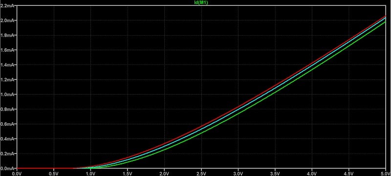
Figure 2. ID vs. VGS with varying VSB (light blue: VSB = 0 V; green: VSB = –0.5 V; red: VSB = 0.5 V).
The threshold voltage with respect to the body effect can be calculated as:
$$V_{th}~=~V_{th0}~+~\gamma \sqrt{2 \Phi_{F}~+~V_{SB}}~-~\sqrt{2| \Phi_{F}|}$$
Equation 5.
where:
Vth0 is the nominal threshold voltage
ΦF is the Fermi potential of the silicon.
The body effect has a big impact on analog designs—it’s very popular to stack transistors on top of one another, which causes the body effect to change the threshold voltages in a non-trivial way.
Channel Length Modulation
In theory, a transistor in saturation should act as a perfect current source with infinite output resistance. In reality, VDS still has an effect on the drain current when the channel pinches off, and so the transistor’s output resistance is large but finite. This is due to a phenomenon called channel length modulation, in which the channel length begins to gradually decrease as the drain voltage increases in the saturation region.
To accommodate channel length modulation, we adjust the drain current equation in saturation to:
$$I_{D}~=~\mu C_{ox} \frac{W}{L}( V_{GS}~-~V_{th})^{2} ( 1~+~ \lambda V_{DS} )$$
Equation 6.
The channel length modulation coefficient, λ, is calculated by:
$$\frac{\Delta L}{L} V_{DS}~=~\lambda$$
Equation 7.
From this, we can calculate the output resistance (ROUT) in saturation to be:
$$R_{OUT}~=~\frac{1}{ \mu \lambda C_{ox} \frac{W}{L} ( V_{GS}~-~V_{th})^{2} }$$
Equation 8.
Subthreshold Conduction
Previously, we defined three transistor operating regions: cutoff, linear, and saturation. In reality, there’s a fourth: the subthreshold region, which has become very popular in ultra-low power analog IC designs.
This region forms because the transistor doesn’t turn off exactly as VGS becomes lower than Vth. Instead, diffusion currents make up a small channel between the source and drain. When VGS < Vth, this diffusion current is non-negligible and has an exponential dependence on VGS. The I-V curve of the resulting subthreshold region is calculated as:
$$I_{D}~=~I_{S}e^{(\frac{V_{GS}}{ \xi V_{T}})}$$
Equation 9.
where:
IS is the specific current of the transistor, and is proportional to \(\frac{W}{L}\)
ξ is a non-ideality factor (> 1 in silicon)
VT is the thermal voltage, and equal to \(\frac{k\text{T}}{q}\).
Mobility Degradation and Velocity Saturation
The drift current within the transistor is determined by the internal electric field, and as transistors have been scaled down, their electric fields have increased rapidly. As it turns out, for short-channel transistors there is a maximum velocity of minority carriers that can be achieved within the transistor. This is known as the saturation velocity.
This limits the current increase with respect to VGS and VDS for certain devices, as eventually their drive current tops out. Furthermore, as electric fields continue to increase, the mobility of these carriers degrades, causing a decrease in drive current at these very high voltages. This short-channel effect is one of many aspects of modern transistor behavior that can’t be predicted by the square-law equations we looked at in the preceding article.
Drain-Induced Barrier Lowering (DIBL)
When VDS becomes large enough, the drain begins to attract negative charge to the surface under the gate, helping the gate to create a channel. The effective threshold voltage decreases as a result, creating a relationship in which Vth is inversely proportional to VDS. This is known as drain-induced barrier lowering, or DIBL for short.
PVT Variations
Variations in process, voltage, and temperature, together referred to as PVT, collectively make up the last non-ideality we’ll discuss.
When transistors are fabricated, manufacturing process variation is inevitable. Process variation can change important transistor characteristics, resulting in different threshold voltages, carrier mobilities, and parasitic capacitances, among other effects. These process variations are often contained within four “corners”: fast-fast, fast-slow, slow-fast, and slow-slow. The corners describe the relative speed of the PMOS and NMOS transistors based on worst-case manufacturing statistics.
Beyond that, variation from one transistor to another is tested via a Monte Carlo analysis that uses models containing statistical data on fabricated transistor parameter variation. Analog designers must utilize both the Monte Carlo and corners methods, as mismatch can have devastating effects on circuit performance.
Finally, operating voltage and ambient temperature also affect transistor performance. These environmental conditions must be checked during the IC design process to ensure the final product operates to specifications.
All images used courtesy of Nicholas St. John