
Modifying the Operation of Digital Components in LTspice
Customizing the device parameters of LTspice's logic gates and flip-flops can help you more accurately simulate these components. This article walks through the specification process and provides some helpful tips.
The first article in this series discussed the underlying electrical structure of LTspice’s logic-gate components, giving particular attention to the thorny question of unused versus logic-low inputs. In this article, we’ll see how adjusting certain of these components’ device parameters allows us to customize their electrical behavior. Our focus will be on the following key parameters:
- Logic voltages.
- Transition times.
- Output impedance.
Figure 1 shows a low-to-high output transition for a basic, two-input AND circuit where all of these parameters are in their default state.
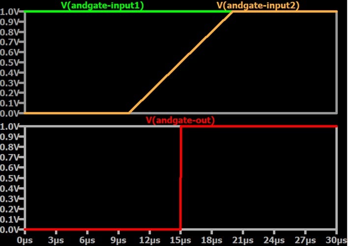
Figure 1. A low-to-high output transition for an LTspice AND gate with default parameters.
The above figure provides us with a baseline for our discussion. Over the course of the article, we’ll examine how modifying different parameters of this AND gate changes our simulation results. Let’s start by looking at the circuit’s logic levels.
Logic Voltages
LTspice’s default voltage scheme for digital components is 1 V logic, with a threshold voltage (Ref) halfway between logic-low and logic-high. In other words, the defaults are:
- Vlow = 0 V
- Vhigh = 1 V
- Ref = 0.5 V
To change one or more of the voltage parameters, right-click the gate symbol. This opens the component attribute editor. Then, add the new voltage specification to the SpiceLine field.
For example, let’s try typing Ref=0.8 into the SpiceLine field (Figure 2). This should change the threshold voltage from its default value (0.5 V) to 0.8 V.
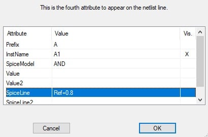
Figure 2. Changing the threshold voltage in LTspice.
Figure 3 shows a low-to-high output transition after the change. As the cursor box shows, the threshold voltage is now at 0.8 V.
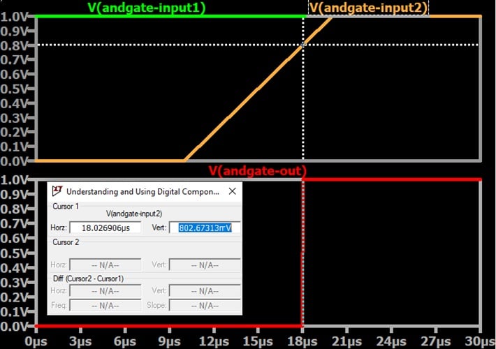
Figure 3. Low-to-high output transition with the threshold voltage set to 0.8 V.
Because we didn’t specify any values for Vhigh or Vlow, they were still at their default when we ran the above simulation. Let’s change that. We’ll give this circuit a logic-low voltage of 0.2 V and a logic-high voltage of 2.5 V.
As Figure 4 shows, these voltages are added to LTspice in exactly the same way as the threshold voltage.
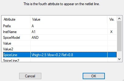
Figure 4. Adjusting the AND gate’s logic-low and logic-high voltages.
Figure 5 shows a low-to-high output transition using the new Vhigh, Vlow, and Ref values.
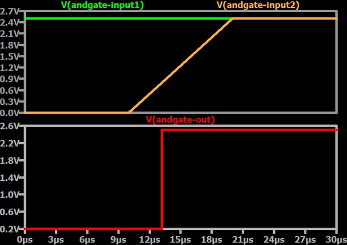
Figure 5. A low-to-high output transition for our example AND gate with Vhigh = 2.5, Vlow = 0.2, and Ref = 0.8 entered in the SpiceLine field.
We’ve now seen how the circuit behaves when custom values are specified for:
- All three voltage parameters (Figure 5).
- None of the three voltage parameters (Figure 1).
- Only the threshold voltage (Figure 3).
But what happens if only the logic-high and logic-low voltages, and not the threshold voltage, have custom values?
According to the LTspice documentation, a logic gate’s input threshold defaults to (Vlow + Vhigh)/2. If the logic-low and logic-high voltages were still at their respective default values of 0 V and 1 V, that would give us the 0.5 V threshold voltage we saw in Figure 1. For the Vlow and Vhigh values we chose above, however, removing the Ref specification gives us the following threshold voltage:
$$(V_{low}~+~V_{high})/~2~=~(0.2~\text{V}~+~2.5~\text{V})/~2~=~1.35~\text{V}$$
This is borne out by the simulation results in Figure 6.
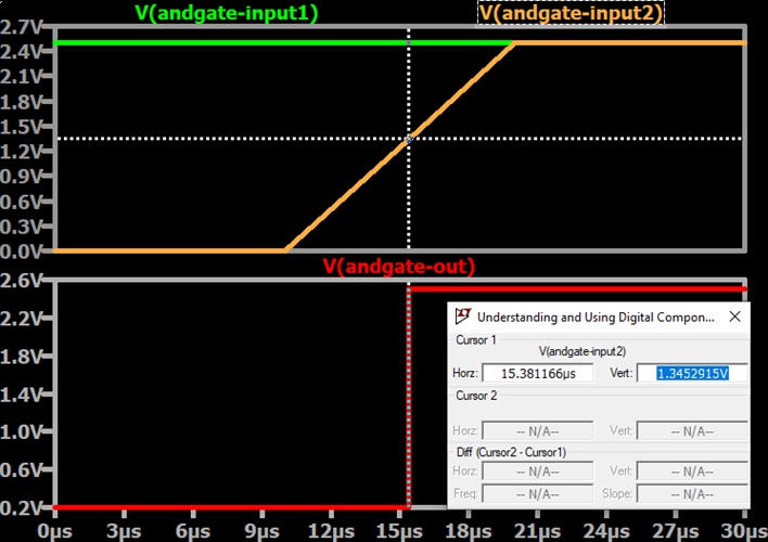
Figure 6. With the Ref specification removed, the threshold voltage defaults to halfway between the logic-low and logic-high voltages.
Next, let’s consider the circuit’s transition times.
Transition Times
By default, the fall time (Tfall) for a digital component in LTspice equals its rise time (Trise). If—as is often the case—you want rise and fall time to be the same, you only need to specify Trise. The default value for Trise is 0, so you probably do want to at least specify a rise time. If you don’t, you’ll have a zero rise time and zero fall time (Tfall = Trise = 0), which will make the transition time for output changes unrealistically short.
Figure 7 shows a zoomed-in output transition for the AND gate setup we used in Figure 5. Values are specified for the logic-high, logic-low, and threshold voltages, but not the rise or fall time.
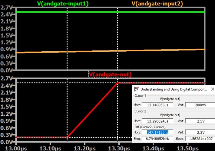
Figure 7. Default rise time for a low-to-high AND gate transition.
I said before that the rise time is zero by default. However, Figure 7 shows that we have a 147 ns rise time—fairly short, but definitely not zero. That’s because it’s limited by the simulation timestep. If I right-click on the simulation command and insert 100p into the Maximum Timestep field, the rise time decreases to the timestep value (Figure 8).
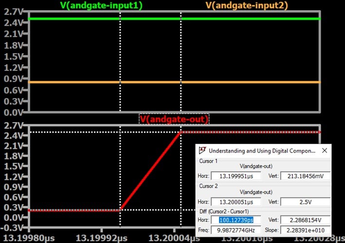
Figure 8. A low-to-high output transition with default rise time and simulation timestep set to 100 ps.
Let’s set the rise time to 50 μs. As we see in Figure 9, the process is identical to how we entered the voltage parameters.
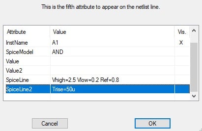
Figure 9. Setting the rise time in the component attribute editor.
Figure 10 shows a low-to-high output transition for the new rise time.
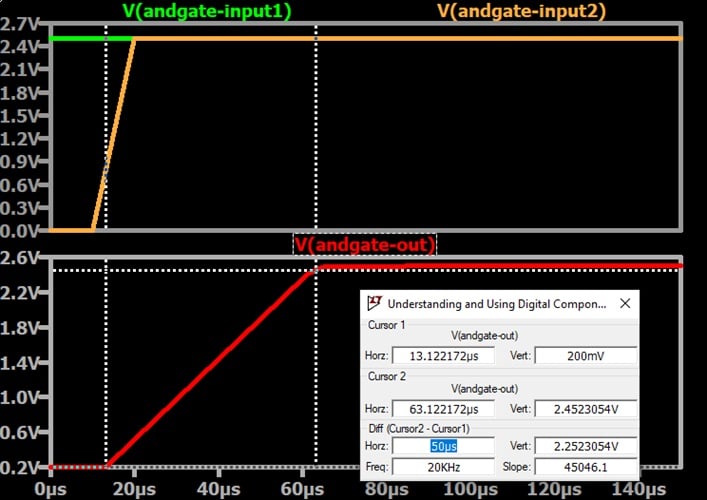
Figure 10. A low-to-high transition with rise time set to 50 μs.
In digital logic circuits, the rise and fall time are often defined as the time required for the voltage to complete 80% of the full transition. However, LTspice defines the rise and fall times for these gates to be 100% of the transition. In theory, then, Figure 10 should show a 2.5 V rise in voltage.
In practice, we can see that the voltage has only risen to 2.452 V after 50 μs—an error of 1.9%. This variation is likely due to the LTspice convergence settings, which control when the simulator decides the resulting voltages and currents are close enough. Changing the convergence settings is beyond the scope of this article.
Output Impedance
The default output impedance is 1 Ω. This is rather low for general-purpose digital logic—a more realistic choice would be something between 10 and 80 Ω. The difference doesn’t matter much when a digital output is connected to a high-impedance, low-capacitance load like a typical digital input.
Sometimes a higher value can improve the simulation. For example, if you want to produce accurate analog waveforms for a circuit in which digital devices must source or sink significant current, a simulation with 1 Ω output impedance might be misleading.
According to the LTspice documentation, you can specify the output impedance of digital components using the Rout parameter. In my experiments with an AND gate and a buffer gate, however, simulation results weren’t consistent with the Rout description provided in the documentation. If you need to increase the output impedance for a digital component, I recommend adding an external resistor, then checking your results to ensure that they make sense.
Up Next
In this article, we discussed how to improve simulations that include digital components by customizing various important parameters. In the next article, we’ll apply our new knowledge to the task of creating a parallel-load shift register in LTspice.
All images used courtesy of Robert Keim


The Rout parameter for the digital gates work, but you can not specify both Trise and Rout. From the A device help: “Note that not all parameters can be specified on the same instance at the same time, e.g., the output characteristics are either a slewing rise time or an RC time constant, not both.”
The output slewing can be specified with Trise and Tfall, or with Tau or Rout and an internal output capacitance, Cout, and/or external load capacitance. You can also provide different rising and falling output resistance Rhigh and Rlow which both default to Rout when not specified.