
Introduction to Thermal Characterization Parameters
In this article, we’ll discuss another group of thermal data, called thermal characterization parameters denoted by the Greek letter Psi (Ψ).
In previous articles in this series, we looked at two important thermal performance metrics of an IC package, junction-to-thermal (or θJA) and junction-to-case (θJC) thermal resistances. We also discussed the test conditions for measuring θJA and how to design for θJC with a heat sink.
In this article, we’ll discuss that thermal resistances cannot give us all the thermal information we need. There is another group of thermal data, called thermal characterization parameters denoted by the Greek letter Psi (Ψ), that can be sometimes even more useful depending on the application.
The Challenge of Measuring a Thermal Resistance
According to the definition, a thermal resistance is the temperature difference between two points divided by the thermal power that flows from one point to the other. Measuring a thermal resistance is not always straightforward. The heat generated in a chip can take many different thermal paths to flow out of the package into the surrounding environment. Unlike the total chip power, the amount of the heat that flows through a certain path cannot be easily determined. This makes measuring the thermal resistance of a path challenging.
To circumvent this problem, we can use an experiment setup that forces almost 100% of the heat generated by the IC to flow through the thermal path of interest. For example, to measure the junction-to-case thermal resistance, we insulate all the surfaces of the system except the package surface in consideration. For the θJC test, this package surface is attached to a copper cold plate. In this way, we can simply measure the temperature difference between the junction and the case and divide it by the chip total power to obtain θJC.
Thermal Resistances Don’t Tell the Whole Story
As discussed above, thermal resistances are measured under specific test conditions. These test conditions might be very different from that of our design. A given thermal resistance can be applied to our design only if its measurement process is similar to our application environment. For example, if we intend to use a heatsink, the θJC parameter can give us an accurate estimation of the junction temperature because a large portion of the heat will flow out of the heatsink as it does in the case of the θJC measurement.
But what about an application without a heatsink?
In this case, the generated heat can flow through the many available thermal paths and θJC won’t be a useful thermal metric. That’s why, in addition to reporting different thermal resistances, manufacturers find it beneficial to characterize the IC thermal performance under conditions similar to that of typical application environments. Thermal characterization parameters, symbolized by the Greek letter Psi (Ψ), provide us with such thermal data.
We’ll discuss below that the Ψ parameters are mathematical constructs rather than true thermal resistances.
The Junction-to-Top Thermal Characterization Parameter (ΨJT)
ΨJT is the temperature difference between the junction and the package top surface divided by the chip “total power”. You might wonder if this isn’t the same as what θJC,Top provided us with. Unlike the θJC,Top test setup, the ΨJT measurement doesn’t restrict the thermal power to flow only out of the top surface. Instead, as depicted below, the heat is allowed to flow normally along all of the available thermal paths.
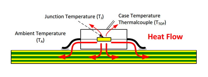
The ΨJT measurement process. Image courtesy of Richtek.
Does this measurement use a standard board? According to the JESD51-12 Guidelines, “the thermal characterization parameters ΨJT and ΨJB (discussed later) are measured by suppliers at the same time and in the same environments as θJA or θJMA”. However, it seems that some manufacturers employ both JEDEC standard boards and user-defined evaluation boards (EVBs) for the Ψ measurements.
Even characterized on a JEDEC type board, ΨJT can give us a more accurate estimation of the thermal performance of an application-specific board. This is because the heat flow is not restricted and it has a partitioning between different paths similar to that of a typical application board.
How Can We Use ΨJT?
Having ΨJT, we can obtain the junction temperature of a device mounted on an application PCB. We only need to measure the case temperature (TC) at the center of its top surface and determine the chip total power (PT). The junction temperature (TJ) can now be obtained as:
\[T_J =T_C + P_T \times \psi_{JT}\]
Keep in mind that θJC rather than ΨJT should be used when application of a heatsink is intended.
ΨJT Is Not a True Thermal Resistance
To obtain ΨJT, the temperature difference between the junction and case is divided by the “total chip power”. With the ΨJT measurement process, the heat is not restricted to flow only out of the package surface. Hence, only a portion of the total thermal power flows from the die to the top of the package.
Since the ΨJT equation divides the temperature delta by the “total chip power” rather than the portion that actually flows out of the top surface, it is considered as a mathematical construct rather than a true thermal resistance. This mathematical construct allows us to characterize the heat flow partitioning that occurs in an application environment with an acceptable accuracy.
Consequently, this makes it possible to accurately estimate the junction temperature of a device mounted on an application PCB. The Greek letter psi is used for thermal characterization parameters to clearly distinguish them from the thermal resistances denoted by the letter theta.
Typical ΨJT Values
ΨJT is a function of both the board characteristics and the airflow conditions. For plastic packages, the ΨJT parameter is a relatively low value under natural convection. This increases with the airflow speed because the airflow forcibly cools the top surface. That’s why the airflow speed is always reported with ΨJT if not measured under natural convection. Some typical values are given in the following table.
| ΨJT for Typical 128 TQFP Package | ||
|---|---|---|
| Air Flow | 1s PCB | 2s2p PCB |
| 0 LFM | 0.7°C/W | 0.5°C/W |
| 200 LFM | 1.8°C/W | 1.4°C/W |
The thickness and thermal conductivity of the plastic mold above die as well as the die size are some of the main factors that affect the ΨJT value. For thin packages, the natural convection ΨJT is typically less than 1 °C/W. A thick package or a very small die can lead to larger ΨJT values in the range of 2 to 10 °C/W. With packages that incorporate an embedded heat slug, the ΨJT value can be very close to zero.
Dependency on PCB Size
A θ parameter can significantly change with the board size. For example, the measured θJA can change from 100 °C/W to as low as 30 °C/W by just increasing the board size from 0.5 in2 to 9 in2. However, with a Ψ parameter, the dependency on the board size will be much smaller as depicted below. This is a key advantage that allows the thermal characterization parameters to offer an accurate estimation of the junction temperature.
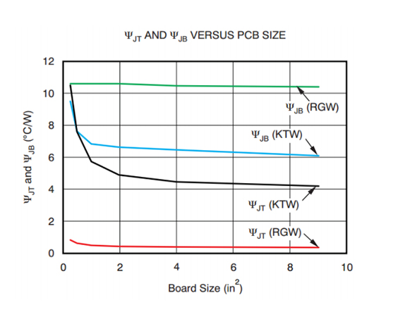
Image courtesy of TI.
Conclusion
Although thermal resistances such as θJA and θJC provide us with some information about the thermal performance of an IC package, they might not be applicable to many application boards.
The complementary thermal information are provided by the thermal characterization parameters denoted by the Greek letter Psi (Ψ). These are actually mathematical constructs rather than true thermal resistances. However, they are very useful numbers that allow us to accurately characterize the thermal performance of an IC on an application board.
To see a complete list of my articles, please visit this page.


