
Introduction to the Inductively-Loaded Class A Power Amplifier
Learn how an inductively-loaded common-emitter stage can function as a power amplifier.
The previous article in this series discussed the challenges and limitations of using a resistively-loaded common-emitter circuit as a power amplifier (PA). In the final section, we learned that many of these challenges can be addressed by using a large inductor as the load of the common-emitter configuration.
In this article, we’ll examine inductively-loaded Class A amplifiers more comprehensively. Let’s begin our study with the basic, inductively-loaded, common-emitter configuration in Figure 1.
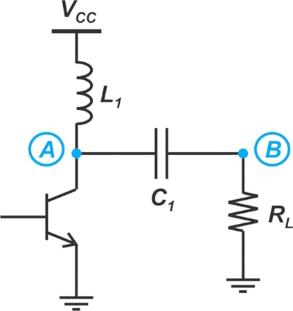
Figure 1. A simple version of the inductively-loaded common-emitter amplifier.
You may have noticed that Figure 1 looks a bit different from the inductively-loaded PA we introduced last time. Unlike that version of the amplifier, which we’ll return to later on in this article, this circuit lacks a matching network. In other ways, this circuit is quite similar:
- The inductor (L1) is large enough to act as an AC open circuit at the frequency of operation. We call such an inductor an “RF choke” (RFC).
- The DC-blocking capacitor (C1) is large enough to be a short circuit at the frequency of operation.
- Power is delivered to a load resistor (RL).
Voltage Swing and Supply Voltage
One interesting feature of the above circuit is that the voltage at node A (VA, or the collector voltage) can exceed the supply voltage (VCC). This is a useful property: with a larger voltage swing, the PA can more easily deliver the high power levels required by its function. Put a different way, an inductively-loaded circuit enables a lower supply voltage for a given voltage swing.
But how can an inductively-loaded stage provide a voltage swing larger than its supply voltage? One possible explanation is that the DC voltage at node A is equal to VCC because the inductor is a short circuit at DC. The RFC carries only a DC current, whose value is determined by the bias circuitry connected to the base of the transistor (not shown in the figure). Since no AC current can flow through the inductor, the AC current of the transistor flows only through RL.
Figure 2 shows two AC equivalent circuit models: one in which the transistor sinks an AC current of ic, and one in which the transistor sources the same AC current.
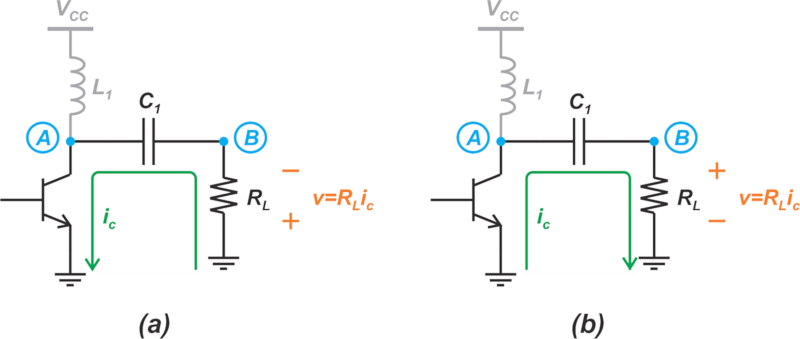
Figure 2. Two equivalent circuit models of an inductively-loaded common-emitter amplifier. In Figure 2(a), the amplifier’s transistor sinks an AC current. In Figure 2(b), the transistor sources an AC current.
In Figure 2(a), the AC voltage at node B is –RLic. With C1 acting as a short circuit, the AC voltage at node A is also –RLic. When we account for both DC and AC components, we observe that the overall voltage at node A goes from VCC to a smaller value of VCC – RLic.
In Figure 2(b), the transistor sources an AC current of ic, and a positive AC voltage appears at node A. In this case, the overall voltage at node A goes from VCC to a larger value of VCC + RLic. We see from this that the collector voltage can exceed VCC.
Another way to reach the same result is to consider the DC voltage across the capacitor C1. In the absence of an AC signal, the nodes A and B in Figure 3 are at VCC and 0 V, respectively. The DC voltage across the capacitor is therefore VCC, with the polarity shown in Figure 3.
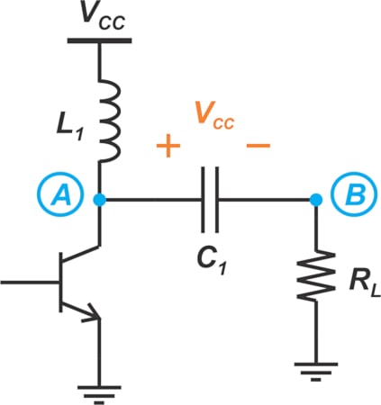
Figure 3. A generic inductively-loaded common-emitter amplifier. Note the polarity on each side of C1.
When the transistor sources an AC current of ic, a positive AC voltage of RLic appears at node B. Accounting for the DC voltage of the capacitor, we observe that the overall voltage at node A is VCC + RLic. Similarly, when the transistor sinks an AC current of ic, the overall voltage at node A drops to VCC – RLic.
Finding the Maximum Voltage Swing
Assume that the transistor has a bias current of ICQ, which is also the DC current that the inductor provides. The maximum AC current that the transistor can source to the load occurs when the overall collector current is almost zero (transistor almost in cutoff). This requires sourcing an AC current of ic,max = ICQ, as illustrated in Figure 4(a).
Using ic,max = ICQ, we find the maximum voltage at node A to be VCC + RLICQ. To have a symmetrical swing, the transistor should also sink ic,max = ICQ. This leads to a minimum voltage of VCC – RLICQ at node A, as we see in Figure 4(b).
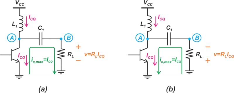
Figure 4. Finding the maximum voltage (a) and minimum voltage (b).
On the other hand, assuming that the transistor’s saturation voltage is zero (VCE(sat) = 0), the minimum collector voltage is 0 V. Therefore, we obtain:
$$V_{CC}~-~R_LI_{CQ}~=~0~ \Rightarrow~ I_{CQ}~=~\frac{V_{CC}}{R_L}$$
Equation 1.
Choosing the bias current according to the above equation ensures maximum symmetrical swing at the output. Figure 4 also shows the range of the current carried by the transistor in the two extreme cases. As we can see, the transistor current can change from 0 to 2ICQ.
To summarize, the collector voltage goes from 0 to 2VCC, and the collector current goes from 0 to 2ICQ. This analysis helps us select a suitable transistor based on its maximum voltage and current limits.
Calculating Maximum Power Efficiency
The maximum power delivered to the load can be calculated as:
$$\begin{eqnarray} P_{L,max} ~=~\frac{1}{2}R_{L}i_{c,max}^2 ~&=&~ \frac{1}{2} ~\times~ R_{L} ~\times~ (\frac{V_{CC}}{R_{L}})^2 \\ ~&=&~ \frac{V_{CC}^2}{2R_L} \end{eqnarray}$$
Equation 2.
The resistively-loaded common-emitter stage discussed in the previous article delivers a considerable amount of undesired DC power to the load. The inductively-loaded circuit delivers only AC power to the load, due to the use of the DC-blocking capacitor. This significantly improves the efficiency, as we’ll see shortly.
The average AC power delivered by the supply voltage is:
$$\begin{eqnarray} P_{cc} ~=~V_{CC}I_{CQ}~&=&~V_{CC} ~\times~ \frac{V_{CC}}{R_{L}} \\ ~&=&~ \frac{V_{CC}^2}{R_L} \end{eqnarray}$$
Equation 3.
We can now use Equations 2 and 3 to calculate the maximum efficiency of the amplifier:
$$\begin{eqnarray} \eta ~&=&~ \frac{ \text{AC Power Delivered to the Load}}{\text{Power Delivered by the Supply}} \\ ~&=&~ \frac{V_{CC}^2 /2R_{L}}{V_{CC}^2 /R_L}~=~50 \% \end{eqnarray}$$
Equation 4.
The amplifier has a maximum efficiency of 50%, meaning that the supply must provide 2 W to deliver 1 W to the load. The remaining 1 W is lost in the transistor. This is a significant improvement over the resistively-loaded stage, which has a maximum efficiency of only 25%.
In practice, however, the achievable efficiency of the inductively-loaded PA can be well below 50%. Figure 5 illustrates how the efficiency changes with the signal amplitude—as we can see, the efficiency is 50% only when the signal swing is at its maximum.
Figure 5 also shows how the three power terms associated with this circuit change with the amplitude of the collector AC current. These three terms are:
- Pcc: Supply power.
- PL: Load power.
- PTran: Transistor power.
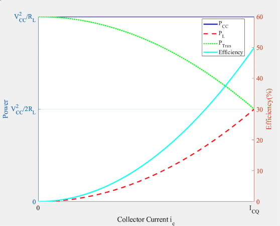
Figure 5. Supply power (blue), load power (red), transistor power (green), and power efficiency (cyan) plotted versus collector current.
As expected, the power provided by the supply (Pcc) is constant. This power is dissipated either in the load (PL) or in the transistor (PTran). When the load power increases, the power dissipated in the transistor drops accordingly. In the absence of an AC signal, zero power is delivered to the load, so the transistor dissipates all the power provided by the supply.
The power dissipated in the transistor gets closer to its minimum value as the signal amplitude increases. From this, we can see that the transistor used in a Class A amplifier is under the most stress when no AC signal is applied. With that in mind, let’s move on to a different version of the inductively-loaded common-emitter stage.
The Need for a Matching Network
Our discussion of inductively-loaded Class A power amplifiers actually began in the preceding article. Let’s go back over a few of the relevant points from that article’s concluding section:
- Achieving maximum output power requires a specific relationship between RL and the bias point of the transistor. This relationship is described in Equation 1 of this article, as well as Equations 3 and 4 of the last one.
- If a given load resistance doesn’t satisfy the above condition, we can use a matching network to transform the actual load (RL) to the optimum load (Req), as shown in Figure 6.
- Matching networks are almost always implemented using reactive components. As a result, the power delivered to the input of the matching network is dissipated in RL.
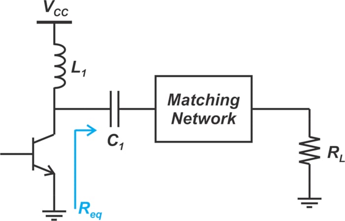
Figure 6. An inductively-loaded common-emitter amplifier that includes a matching network.
One common way to implement the matching network is to use a transformer, as illustrated in Figure 7.
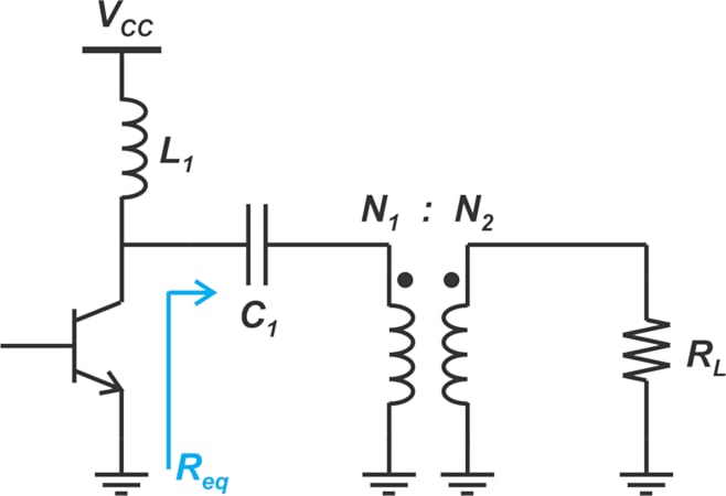
Figure 7. An inductively-loaded common-emitter amplifier that uses a transformer as a matching network.
In the above figure, we have:
$$R_{eq} ~=~ \big ( \frac{N_1}{N_2} \big )^2 R_L$$
Equation 5.
where N1 and N2 are the turns, meaning the number of windings on each side of the transformer. By using an appropriate turns ratio, we can make the load resistance RL appear either larger or smaller at the collector, as needed.
The following example, inspired by a problem from “RF Microelectronics” by B. Razavi, should help you better understand how the transformer can change the power transistor’s maximum voltage and current requirements.
Example: Finding the Turns Ratio of a Transformer
We intend to use the circuit in Figure 7 to deliver 4 W to a 50 Ω load. If the supply voltage is 2 V and the circuit operates at its maximum efficiency, what is the required turns ratio for the transformer?
To determine this, we first find the equivalent load resistance (Req) that maximizes the output power. Applying Equation 2 with Req as the load resistance of the stage, we obtain:
$$P_{L,max} ~=~ \frac{V_{CC}^2}{2R_L} ~\Rightarrow~ 4~=~\frac{2^2}{2R_{eq}}$$
Equation 6.
which results in Req = 0.5 Ω. Having RL and Req, we can now use Equation 5 to find the required turns ratio:
$$0.5 ~=~ \big ( \frac{N_1}{N_2} \big )^2 ~\times~ 50 ~\Rightarrow~ \frac{N_2}{N_1}~=~10$$
Equation 7.
Delivering 4 W to a 50 Ω load requires:
- A peak-to-peak voltage swing of 40 V.
- A peak current of 400 mA through the load.
Due to the transformer’s operation, the peak-to-peak voltage swing at the collector is 40/10, or 4 V, which is theoretically possible with a 2 V supply. However, ic,max = 0.4 × 10, making the peak AC collector current 4 A!
When the collector voltage is at its minimum, the transistor sinks twice ic,max. Therefore, 8 A is the maximum current that the transistor in this example can carry without being damaged.
Up Next
I hope that this article, taken together with the previous one, has helped you to understand how Class A power amplifiers function. In the next article, we’ll build on this knowledge by introducing some practical PA design techniques. In particular, we’ll learn how to estimate and analyze a power amplifier’s load-pull contours, using a Class A amplifier for our example calculations.
Featured image used courtesy of Adobe Stock; all other images used courtesy of Steve Arar


Good article!
But is not clear how big is needed even inductor as capacitor in this circuit. Which parameters we can choice to evalute it porpoerly? There is a loto of DIY projects on web, but never is showed how to get a compromissed performance, or normally nobody talks about que audio quality concerned to bad choices about those components.
Can you clear this issues next time?