
How to Simulate a Bidirectional Voltage-Controlled Current Source
Learn about simulating an interesting current source built around an op-amp and an instrumentation amplifier.
Learn about simulating an interesting current source built around an op-amp and an instrumentation amplifier.
This article, part of AAC’s Analog Circuit Collection, examines the operation and dynamic performance of a current source built around an op-amp and an instrumentation amplifier.
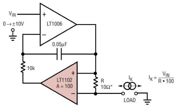
In a previous article, I introduced an interesting current-source topology I found in an old Linear Tech app note. As you can see in the schematic below, the instrumentation amplifier in the op-amp’s feedback loop causes the op-amp’s output to generate a load current that is independent of the load resistance.
The circuit offers high precision and good dynamic performance, and it provides a pleasantly straightforward relationship between the controlling input voltage and the generated load current.
Before we go into the operation and dynamic performance of the topology, we'll go over what the circuit looks like in LTspice.
Related Information
For more background information, please check out these resources:
- The Basic MOSFET Constant-Current Source
- Learn Analog Circuits: Types and Applications of Current Mirrors
- The Howland Current Pump
- Need a Current Regulator? Use a Voltage Regulator!
The LTspice Implementation
My LTspice version of the circuit is shown below.

- Fortunately, LTspice includes macromodels for the exact components used in the original design. If you want to incorporate different amplifiers into this circuit, I highly recommend that you choose parts that have accompanying macromodels. My instinct tells me that this is the sort of circuit that should be simulated before it is built.
- As you can see, pin 2 and pin 7 of the LT1102 are currently disconnected. This configures the part for a fixed gain of 100, and the resulting transfer function is ILOAD = VCNTRL/(R1×100). If you connect pin 2 to ground and pin 7 to pin 8, the gain of the LT1102 will be 10, in which case the transfer function becomes ILOAD = VCNTRL/(R1×10).
- The control voltage shown in the schematic above is a ramp that extends from –5 V to +5 V in a period of 100 ms. This control voltage will be used to demonstrate the low-frequency performance of the circuit.
Low-Frequency Operation
The plot below shows you how the current source reacts to a slowly changing input voltage. As expected, the load current increases linearly from –5 mA to +5 mA.

We can estimate the circuit’s low-frequency precision by applying the mathematical transfer function to the control voltage and then plotting the difference between the theoretical output current and the simulated output current.

So we’re looking at an error of approximately 45 µV, with only minor variation over the –5 V to +5 V input-voltage range. This seems quite good to me, considering the various nonidealities that are present in the two amplifiers (although I don’t know how exactly these nonidealities are incorporated into the macromodels).
This error assumes, however, that R1 is exactly 10 Ω. Since R1 (in conjunction with the gain of the instrumentation amplifier) determines the constant of proportionality between the control voltage and the output current, you have to use a very-low-tolerance resistor if you want the actual transfer function to replicate the theoretical transfer function. On the other hand, if this is for a one-off project or a prototype or some such, you can simply measure the resistance of R1 and then generate your control voltage based on the measured resistance value instead of the ideal value.
I ran a few more simulations with different values of load resistance, and the general trend is for error to decrease as load resistance increases. For example, the error at RLOAD = 600 Ω is approximately 19 µV.
Dynamic Performance
This current source is based on negative feedback, which inherently involves some delay associated with the settling behavior, and the amplifiers have bandwidth and slew-rate limitations. Consequently, we shouldn’t expect this circuit to translate rapid input-voltage variations into equally rapid output-current variations.
However, all things considered, the output has a good ability to reproduce abrupt changes in the control voltage, and it’s also important to note that these abrupt changes do not create excessive ringing.
To simulate the dynamic response, I changed the voltage source to a pulse that transitions from 0 V to 5 V with a rise/fall time of 1 µs. The input signal is shown below, along with the resulting output-current signal.

Dynamic performance with RLOAD = 600 Ω.
The Linear Tech app note describes this circuit’s dynamic response as “well controlled,” and I would agree. The output current increases and decreases in a uniform way, and a slope of 0.65 mA/µs is nothing to complain about. There is no ringing on the rising or falling edge, and the amplitude of the overshoot is very low.
One interesting detail that I noticed is shown in the following plot. After the falling edge, the output current takes a (relatively) long time to return to the expected value of 0 mA.

Recovery behavior with C = 0.05 µF.
You can shorten this recovery time by reducing the value of the capacitor, but this leads to a transient response that is less “controlled”:

Recovery behavior with C = 0.005 µF.
Conclusion
With the help of LTspice, we’ve gathered some useful information about the performance of the "Jim Williams current source" (as explained in the previous article, this is not the official name, but it’s more engaging than the name used in the app note—“Voltage Programmable, Ground Referred Current Source”).
It would be interesting to see how this circuit performs with amplifiers that are a bit more “modern.” If you do any simulating or bench testing with a customized implementation, don’t hesitate to share your thoughts and experiences in the comments section below.


Hey Robert, really enjoying this article series! A pleasure to read. Thank you. I’m probably going to play with this one in simulation and perhaps on the breadboard with different opamps and post some “feedback” if I do 😉
I’m working on a bidirectional current source for driving two LEDs (for user interface indication of positive and negative voltages) and they couldn’t have landed in my inbox at a better time! I’m in a bit of a tricky space since I can’t draw the actual LED current from the negative rail (it should all come from a +5V buck converter) so it’s a bit of a wonky challenge.
Not sure if this was intentional, but the first figure in this article looks like the Howland Current Pump scheme. Was it perhaps supposed to be the current source from the Jim Williams app note?
Excellent article,
I was recently refurbishing an old 1960’s 2 transistor tachometer for a car
It converted pulse time trails into an analog readout by integrating the output of an RC network in a monostable configuration.
This current source would have been useful set up for experimenting with capacitor time discharge for the monostable. (Probably overkill, but a really interesting exercise)
Thanks for the article - really useful AND interesting
The circuit shown above is a Howland current pump, not the Williams current source circuit using an instrumentation amplifier. That confused me for a while.