Designing L-type Matching Networks Using Series and Parallel RC and RL Circuits
Learn about l-type impedance matching equations through the quality factor (Q factor) of RC and RL circuits and the series-parallel conversion of these circuits.l-
In the previous article in this series, we learned how passive impedance matching networks can be designed using the Smith chart. Rather than using this graphical method, it is also possible to follow an analytical approach and use some equations to obtain the desired matching network.
First, before diving into the impedance matching equations, we need to learn about two basic concepts: the quality factor of RC and RL circuits and the series-parallel conversion of these circuits.
Quality Factor Definitions for RC and RL Circuits
The term quality factor, denoted by Q, can be defined in a number of ways. When talking about an energy-storing device (i.e. a capacitor or inductor), Q shows how close to ideal our energy-storing device is. For example, an ideal capacitor doesn’t dissipate any energy and should have an infinite Q. Now, consider a real-world capacitor modeled as a parallel RC circuit (Figure 1(a)).
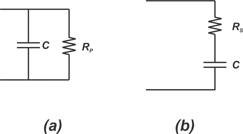
Figure 1. A parallel RC circuit (a) and a series RC circuit (b).
In this case, the resistor can represent the resistive losses of the actual capacitor. For a parallel RC circuit, Q can be defined as:
\[Q_P=\frac{R_P}{\frac{1}{C \omega}}\]
Equation 1.
Next, let’s see if this equation makes sense. In the circuit diagram of Figure 1(a), when RP goes to infinity, we’re left with an ideal capacitor (for which Q = ∞). This is consistent with the above equation that produces an infinite Q in the limit of infinite RP.
Now consider a capacitor with a series resistor RS, as shown in Figure 1(b). In this case, Q is defined as:
\[Q_S=\frac{\frac{1}{C \omega}}{R_S}\]
Equation 2.
In the series RC circuit, the ideal energy-storing device is obtained for RS = 0. This is also consistent with Equation 2, which produces an infinite Q in the limit of RS = 0. In Equation 1, Q is defined as the ratio of the undesired impedance (RP) to the impedance of the capacitive component, whereas Equation 2 defines Q as the ratio of the impedance of the capacitive component to that of the dissipative component. Using your intuition, how do you think the quality factor of a parallel RL (Figure 2(a)) and series RL (Figure 2(b)) is defined?
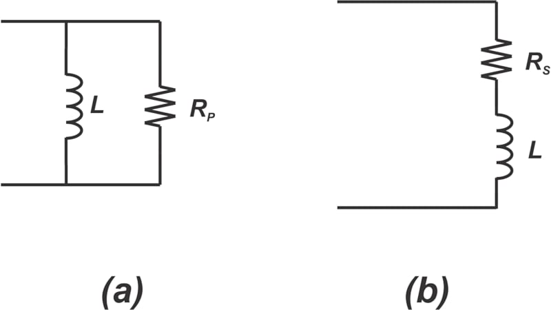
Figure 2. Parallel RL circuit (a) and series RL circuit (b).
The quality factor of a parallel RL circuit (QP) and series RL circuit (QS) are respectively shown in Equations 3 and 4:
\[Q_P = \frac{R_P}{L \omega}\]
Equation 3.
\[Q_S=\frac{L \omega}{R_S}\]
Equation 4.
Again, note that as RP goes to infinity, Equation 3 produces an infinite Q; and as RS goes to 0, QS tends to infinity. Keeping these extreme cases in mind, you can easily remember the correct equation for each configuration.
RL and RC Circuit Series and Parallel Conversion
A key step in designing an impedance-matching network is to transform a series connection of components to their equivalent parallel connection or vice versa. This is usually referred to as the series-parallel conversion or shunt-series transformation in the RF literature. As an example, consider the series RL circuit depicted in Figure 3(a) below.
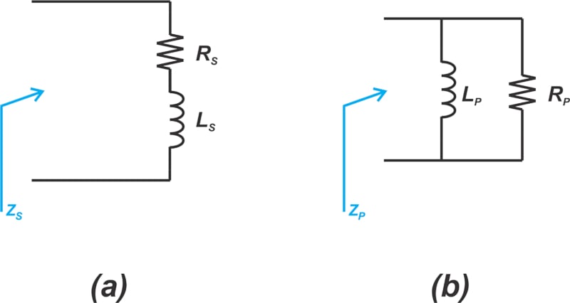
Figure 3. A series RL circuit (a) and its equivalent RL circuit (b).
At a single frequency, we can model the series RL circuit by an equivalent parallel RL circuit, as shown in Figure 3(b). By equating the input impedance of these two circuits (ZS=ZP), we can find the component values of the parallel circuit in terms of those of the series circuit. This produces the following set of equations:
\[R_P = R_S (1+Q^2)\]
Equation 5.
\[L_P = L_S (\frac{1+Q^2}{Q^2})\]
Equation 6.
Where Q denotes the quality factor of the circuits (Equations 3 and 4 from the previous section). Note that the Q of the series RL circuit (QS) and that of the parallel equivalent circuit (QP) are the same at the frequency where the two circuits produce the same impedance. As a result, Equations 5 and 6 use the symbol Q rather than QS or QP to represent the quality factor. The above equations can be used to convert from the series to the parallel circuit or vice versa. Similarly, we can derive mathematical equations to convert a series RC circuit (Figure 4(a)) to its equivalent parallel circuit (Figure 4(b)) and vice versa.
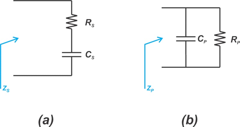
Figure 4. Example series RC circuit (a) and its equivalent parallel circuit (b).
Equation 5 also applies to the series-parallel conversion of RC circuits. However, keep in mind that now the Q term is the quality factor of the RC circuits (Equations 1 and 2). The capacitor values are related by the following equation:
\[C_P = C_S (\frac{Q^2}{1+Q^2})\]
Equation 7.
The equations presented above have simple interpretations. Equation 5 shows that the parallel equivalent resistance is greater than the corresponding series resistance by a factor of (1+Q2). Also, assuming that the Q is relatively large, the reactive components of both the series and parallel circuits are of almost the same value. Let’s look at an example to clarify the above discussion.
Example 1: Input Impedances of a Parallel and Series RC Circuit
Assume that the input impedance of an RF block can be modeled by a parallel RC circuit with RP = 50 Ω and CP = 3.88 pF, as depicted in Figure 5 below.
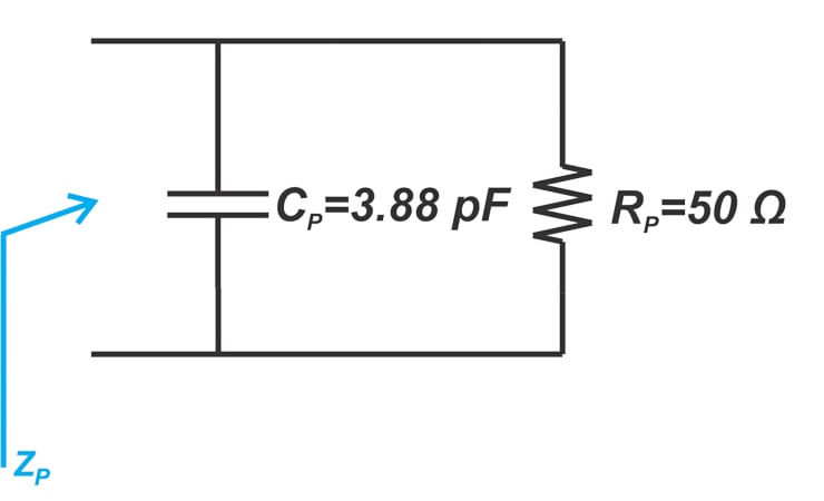
Figure 5. Example parallel RC circuit RP = 50 Ω and CP = 3.88 pF.
Find the equivalent series RC circuit at 1 GHz.
By applying Equation 1, the Q of the parallel RC circuit is found:
\[\begin{eqnarray}
Q_P &=& R_P C_P \times \omega \\ &=& 50 \times 3.88 \times 10^{-12} \times 2 \pi \times 1 \times 10^{9} \\ &=& 1.225
\end{eqnarray}\]
Substituting Q = 1.225 into Equations 5 and 7, we have:
\[R_S = \frac{R_P}{1+Q^2}=\frac{50}{1+1.225^2}= 20 \text{ } \Omega\]
\[C_S = C_P \frac{1+Q^2}{Q^2}=3.88 \times 10^{-12} \times \frac{1+1.225^2}{1.225^2}= 6.47 \text{ } pF\]
The equivalent series circuit is shown in Figure 6.

Figure 6. Equivalent series circuit with RS = 20 Ω and CS = 6.47 pF.
The input impedance of the two circuits is plotted in a polar form in Figure 7.
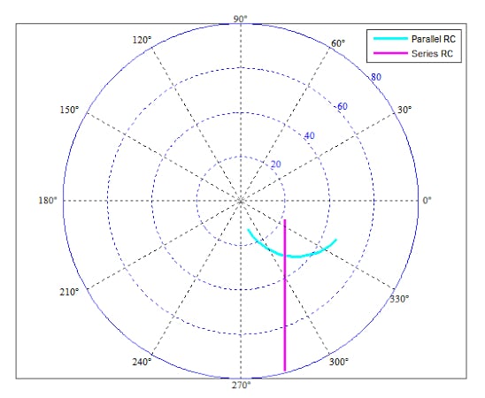
Figure 7. The input impedance of a parallel and series RC circuit.
A polar plot allows us to display the effect of both real and imaginary parts of the impedances by a single curve.
Note that the impedances are equal only at a single frequency (at the intersection of the two curves that correspond to 1 GH in our example). At this frequency, the input impedances work out to ZS = ZP ≃ 20 - j24.12 Ω. If we consider a narrow frequency range of around 1 GHz, we can assume that the two circuits have identical input impedances.
Example 2: Designing a Matching Network Using Series-parallel Conversion
Use the results of the previous example to design a matching network that transforms RL = 50 Ω to 20 Ω at 1 GHz.
In the previous example, we saw that a parallel RC circuit with RP = 50 Ω and CP = 3.88 pF is equivalent to a series RC circuit with RS = 20 Ω and CS = 6.47 pF. Based on this information, we can place a 3.88 pF capacitor in parallel with RL = 50 Ω to produce the desired 20 Ω resistive part. We only need to eliminate the reactive component from the equivalent series capacitor (CS). The reactance of CS = 6.47 pF is about -j24.12 Ω at 1 GHz. We can use a series inductor of 3.84 nH to produce a reactance of about +j24.12 Ω. This series inductor cancels the reactance of CS, leaving us with a purely resistive impedance of 20 Ω. The final matching network is shown in Figure 8.
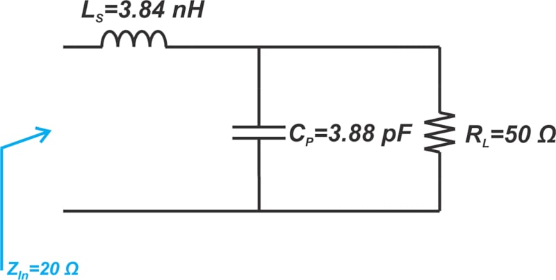
Figure 8. Example matching network diagram.
Now that we have established the concepts of quality factor and series-parallel conversion, we can discuss the analytical method of designing impedance-matching networks.
L-type Impedance Matching of Two Resistive Terminations
Two-element lossless matching networks, known as L-sections, are widely used in RF circuits. The circuit we designed in the above example (Figure 8) is actually an L-type matching network. Let’s now see how we can design these matching networks for arbitrary load (RL) and source (RS) impedances. To transform RL to RS, we can imagine two different types of solutions, as shown in Figure 9 below.
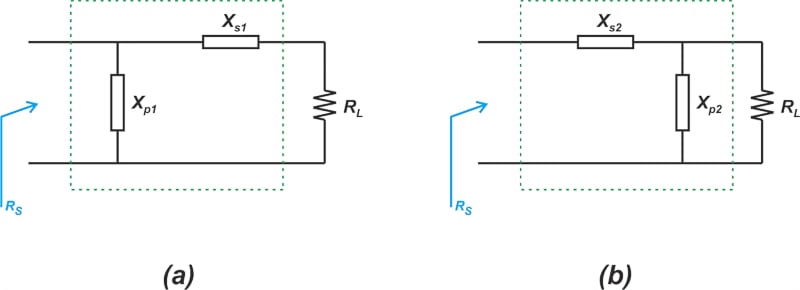
Figure 9. Example circuits of arbitrary load (RL) and source (RS) impedance solutions.
In the above figure, the X components denote the reactance of the matching elements. For a given RL and RS, only one of the above solutions can be used. In order to determine the right choice, let’s apply the series-parallel conversion. This produces the following equivalent diagrams in Figure 10.
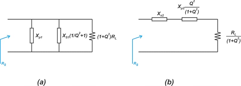
Figure 10. Two example equivalent diagrams after applying series-parallel conversation to Figure 9.
The resistive part of the circuit in Figure 10(a) is (1 + Q2) times greater than RL, whereas the resistive part of the circuit in Figure 10(b) is equal to RL divided by (1 + Q2). This means that the circuit in Figure 9(a) transforms RL to a higher resistance; however, the circuit in Figure 9(b) transforms RL to a lower resistance. Therefore, when designing L-sections, the series component should be connected to the termination that has a smaller resistance. Consequently, the parallel component of the L-section should be connected to the termination that has a larger value. With the insight we’ve developed so far, we can pursue the following steps to design an L-section:
1. Name the termination with a larger value RHigh and the other one RLow. And use the following equation to calculate the quality factor of the circuit:
\[Q=\sqrt{\frac{R_{High}}{R_{Low}}-1}\]
Equation 8.
2. Place a series reactive element next to RLow and a parallel component next to RHigh. This produces two subnetworks: one series and the other one parallel, as shown in Figure 11.
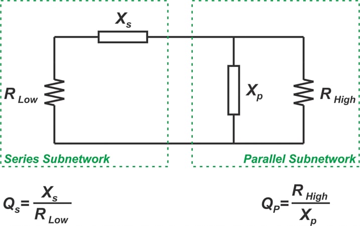
Figure 11. Example series and parallel subnetworks.
The above figure also provides the Q equation for the series and parallel subnetworks. At the frequency where the match occurs, the quality factor of the subnetworks is the same and equal to that given by Equation 8, i.e. QS = QP = Q.
Note that, in the above circuit diagram, the input voltage source is actually zeroed because, here, the aim is to provide a match between the load and source impedances. The final circuit diagrams actually include a voltage source in series with either RLow or RHigh (Figure 12 below shows the final circuits).
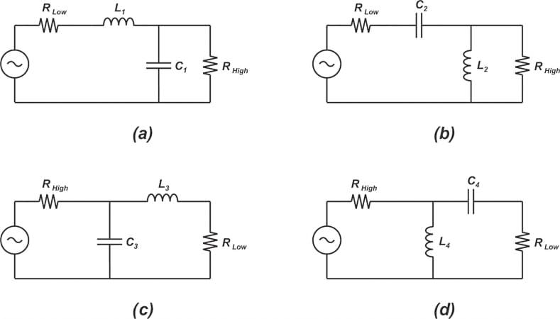
Figure 12. Examples for matching two resistive impedances.
3. Having QS, QP, and the termination resistances, we can find the reactance values XS and XP. Finally, the inductor and capacitor values are calculated at the frequency of interest.
Note that XS and XP can be a capacitor or an inductor; however, they are not of the same type. In other words, to transform a purely resistive load to another purely resistive impedance, we need an L-section consisting of an inductor and a capacitor. L-sections consisting of either two capacitors or two inductors cannot provide a match between two resistive impedances. Therefore, as shown below in Figure 12, there are a total of four different options when providing a match between two resistive impedances.
Let’s look at an example.
Example 3: Designing and Transforming a Matching Network Using Q Factor
Design a matching network that transforms RL = 10 Ω to 50 Ω at 1 GHz.
By applying Equation 8, the required quality factor is found:
\[\begin{eqnarray}
Q &=& \sqrt{\frac{R_{High}}{R_{Low}}-1} \\ &=& \sqrt{\frac{50}{10}-1}=2
\end{eqnarray}\]
Placing the series component next to RL (the lower resistance), we obtain the following L-sections (Figure 13):
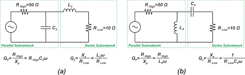
Figure 13. L-section diagrams after placing a series component next to RL.
With the circuit in Figure 13(a), we have:
\[Q_S = \frac{X_S}{R_{Low}}=\frac{L_3 \omega}{R_{Low}}=2\]
\[Q_P = \frac{R_{High}}{X_P}=R_{High}C_3 \omega=2\]
At 1 GHz, the above equations produce L3 = 3.18 nH and C3 = fc6.37 pF. For the circuit in Figure 13(b), we have the following set of equations:
\[Q_S = \frac{X_{S}}{R_{Low}}=\frac{1}{R_{Low} C_4 \omega}=2\]
\[Q_P = \frac{R_{High}}{X_{P}}=\frac{R_{High}}{L_4 \omega}=2\]
At 1 GHz, the component values are C4 = 7.96 pF and L4 = 3.98 nH.
L-type Matching Network Design Summary
L-type matching networks can be designed using either the Smith chart-based graphical method or some simple equations. In this article, we derived the equations for the analytical method and looked at some examples. A key step in the design of impedance-matching networks is the series-parallel conversion of RL and RC circuits. It’s worthwhile to mention that series-parallel conversions are also helpful in analyzing component models to find the combined effect of different kinds of losses.