
Designing a Wideband Analog Voltage and Current Meter
Design a wideband analog multimeter to measure AC voltages and currents from 20 Hz to 1 MHz with a selectable sensitivity from 1 mV to 100 V, while the ammeter has a selectable current sensitivity of 10 mA to 10 A.
It may be surprising to offer a purely analog meter when digital meters are now so widely used. However, it isn’t well-known that digital meters have analog circuits preceding the analog-to-digital converter (ADC). Wideband analog voltmeters, with frequencies from below 20 Hz up to 200 kHz, have been widely used in the past and are still very useful.
Key Specifications for a Wideband Analog Meter
With modern operational amplifiers (op amps), the design of our analog meter can be greatly simplified. This design provides a flat bandwidth of 20 Hz to 1 MHz (-1 dB at 10 Hz) using reasonably-priced components.
It is not difficult to add the capability of measuring currents in circuits in which the insertion of a resistance of 0.1 Ω at the grounded end does not reduce the current significantly. If the meter is battery-operated or of safety Class 2 construction, the grounded connection does not have to be an actual ground.
The six voltage ranges are 1, 10, 100 mV, and 1, 10 ,100 V full scale, while the four current ranges are 10, 100 mA, and 1, 10 A full scale. The design incorporates a wide-band peak detector, whose sensitivity can be switched to read the peak voltage or the root mean square (RMS) voltage of a sine-wave signal.
There is a provision to insert external filters to provide special frequency responses. This feature also allows the meter to be used as two separate amplifiers with switched variable gain.
The instrument will run from two 9 V batteries or a 9-0-9 V mains power unit. The current drain is below 25 mA for each battery (without any light-emitting diode (LED) indicators), so long life can be predicted.
Analog Meter Project—General Description
The block diagram of the instrument is shown in Figure 1.

Figure 1. Block diagram of the wideband analog meter.
The input attenuator/current mode selector is necessary since we want to measure voltages up to 100 V, and they can’t be applied directly to the amplifier. The current mode is selected so that there is no switch contact in series with the current-sensing resistor, thus eliminating a potential source of error. The small price to pay is that a separate connector is required for current-mode operation.
Using Two Op Amps to Reach Gain
The amplifier requires a gain of around 1000 (60 dB) to give a full-scale reading for 1 mV input. This is achieved by using the two op amps in the LM4562, with gains of 31.62 each. The LM4562 is actually intended for hi-fi preamps, so it has low noise and low distortion, together with a wide bandwidth. It isn’t so hot on offset voltage, but that can be overcome in this application.
Since there are two amplifier stages, it is easy to provide connectors and switching so that other circuits can be inserted between the two amplifiers, and they can also be used as independent amplifiers if a further connector is added at the output of the second amplifier.
Choosing Your Detector: Half-wave, "True-RMS," and Full-wave Peak
An important decision has to be made concerning the type of detector provided to turn the amplified signal into DC for operating either a digital display or a pointer instrument. The simplest detector is a half-wave average type, which tells us little about the signal and may hide a significant voltage excursion in the undetected half-cycle.
At the other end of the complexity scale is the "true-RMS" detector, labeled ‘true’ to distinguish it from an average detector whose gain has been tweaked to read the RMS value of a wave signal but not of all others. This is good if you want to know the RMS value of the signal, but the only reasonably-priced device is the AD736, which is limited to 200 kHz, whereas the amplifier works up to 1 MHz and beyond.
The third type of detector is the full-wave peak detector, and this can be constructed at a reasonable price. It is very often that the peak value of a signal needs to be measured, as it may indicate that something in the signal chain is overloaded and peak-clipped. It is also easy to find the RMS value of a sine-wave signal (even with up to about 10 % distortion) by dividing the peak value by 1.4 or multiplying by 0.7, as long as the waveform isn’t significantly clipped. This is easily arranged because it requires a 3 dB attenuator to be switched in.
Another simple attenuator interpolates between the 20 dB (10 times) steps of the range switch, which allows all indications above 0.5 mV on a pointer instrument to be in the upper half of the scale. Both attenuators can be applied.
Searching for published full-wave peak detectors that work up to 1 MHz proved unfruitful, but by merging techniques from two unsuitable detectors, a solution has been found, using another LM4562 and two RF bipolar transistors BF140. Other transistors with similar or better characteristics can, of course, be used, but general-purpose transistors such as BC547/847 are not suitable.
Project's Circuit Design Aspects
For this experiment, the blocks are described individually, with their schematics (except for the amplifiers), which use a dual op amp and a 2-pole switch, thus, separating them would be confusing. The whole schematic is too big to be legible if shown on a single page. The power supply connections at the op amps are shown only as V+ and V– and in the power supply block to avoid too many long wires.
The Input Attenuator and Current-mode Switch
The schematic for the input attenuator and current-mode switch is shown in Figure 2.

Figure 2. Input attenuator and current-mode switch [click image to enlarge].
The switch is shown in the highest sensitivity position. Beginning at the lower position and moving clockwise, the switch steps are current mode (10 mA), 100 V, 10 V, and 1 V.
The current-sensor resistor (and all resistors used in the project unless otherwise stated) should have ±1% tolerance, so it is not a cheap component but affordable. An alternative is to use a 0.15 Ω resistor with another value in parallel, chosen to give close to 0.1 Ω. It should not be wirewound unless metal-cased because otherwise, the inductance might introduce error at high frequencies: 100 nH is 628 mΩ at 1 MHz.
Note that the current sense resistor is connected as closely as possible across the input connector so as not to introduce extra resistance. There is also no DC blocking capacitor in series for the same reason. If a component with a power rating of 1 W or more is used, any DC component less than 10 A should not cause a problem.
C2 should be a polyester film capacitor of 250 V rating or higher if you use higher DC voltages.
The trimmer capacitor is there to adjust the attenuations to be correct at high frequencies. These values worked for me, but the capacitances are very construction-dependent, so you may need different values or configurations.
First and Second Amplifiers and Range Switch
The schematic is shown in Figure 3.
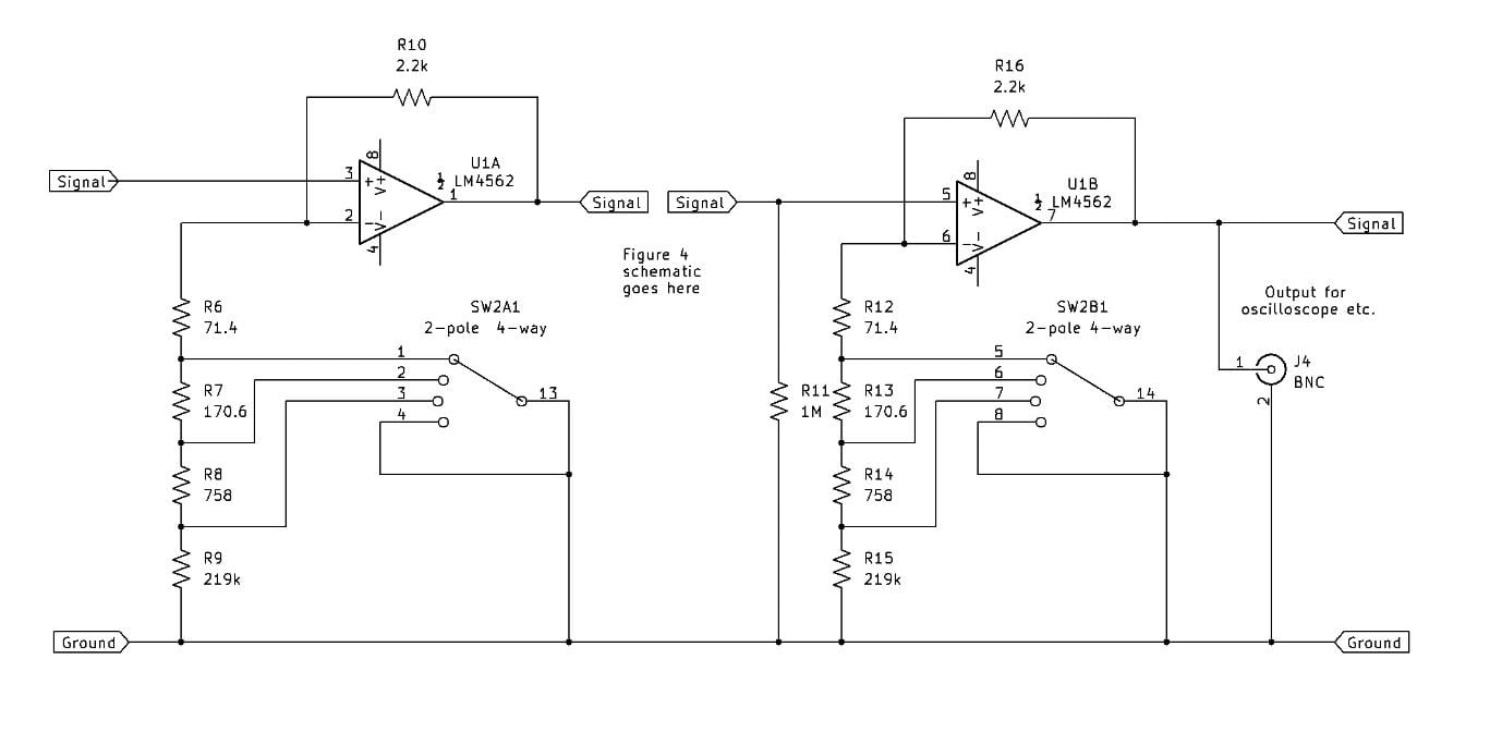
Figure 3. First and second amplifiers and range switch [click image to enlarge].
The switching is arranged so that there are no unused resistors attached to the signal circuit; they are attached to the ground. The switching for the 3 /10/13 dB attenuators and ‘External filter’ are covered in the next section.
The switches are shown in the 1 V position. Each step changes the gain by 10 dB on each switch pole, giving 20 dB steps (10 times).
The low value of the feedback resistors R10 and R16 is the key to getting wide bandwidth. They need to be as near 2.2 k Ω as possible, which may mean selecting from several components.
R5 and R10 could be E96 series value 71.5 Ω, or 82 Ω || 560 Ω (|| means ‘in parallel’). R6 and R11 are 180 Ω || 3.3 kΩ. R7 and R12 are 820 Ω || 10 kΩ. Other combinations are obviously possible. Additionally, R8 and R13 can be 220 kΩ.
It is necessary to get as close to the required values as possible because the instrument's accuracy depends on it. Preset resistors should be avoided, if possible, or high-quality components should be used; otherwise, calibration stability will suffer.
Note that using the 2.2 kΩ and 220 kΩ resistors for feedback gain setting produces a non-inverting amplifier with a gain of 1.01 (0.086 dB), which is close enough to 1.
Additional Attenuators and External Filter Connectors
The 3 dB (peak-to-RMS sine wave) and 10 dB (scale magnifier) attenuators, and the external filter switches, are shown in Figure 4.
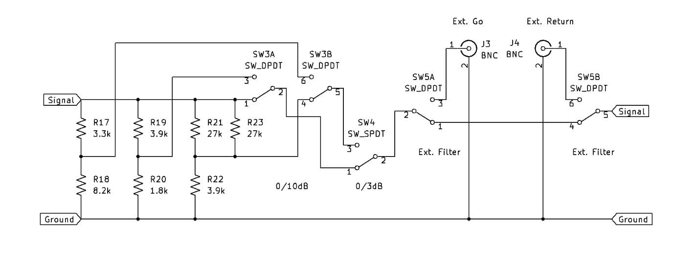
Figure 4. Diagram of 3/10/13 dB attenuators and external filter connectors [click image to enlarge].
As before, it is necessary to measure the resistors and choose those closest to the required values. It helps that, in this case, E12 preferred values can be used at the cost of one extra resistor for the -13 dB network.
It’s useful to examine how well the E12 series resistors give the required attenuation. Table 1 shows the results.
Table 1. Error as a function of attenuation ratio.
|
Attenuation |
Attenuation Ratio |
Upper Arm Resistor |
Lower Arm Resistor |
Ratio |
Error % | Error dB |
|---|---|---|---|---|---|---|
| 3 | 0.7071 | 3.3k | 8.2k | 0.7130 | -0.84 | -0.062 |
| 10 | 0.3162 | 3.9k | 1.8k | 0.3158 | 0.14 | 0.012 |
| 13 | 0.2236 | 13.5k | 3.9k | 0.2241 | -0.24 | 0.021 |
| 3dB fix | 0.7071 | 3.382k | 8.2k | 0.7080 | -0.12 | -0.011 |
Using measured-value resistors, the error can be minimized by adding a low-value resistor in series with whichever resistor is too low. For example, if the resistors for 3 dB were both exactly 3.3 kΩ and 8.2 kΩ, the error could be fixed by adding 82 Ω in series with the 3.3 kΩ.
It’s quite convenient to use toggle switches in this network, but of course, slide or rotary switches could be used.
Peak Detector and Meter
The peak detector is shown in Figure 5.

Figure 5. A diagram showing the peak detector [click image to enlarge].
It has three features that secure wide bandwidth:
- The resistor values are much lower than usual in these circuits
- Schottky diodes are used in the first stage
- Two emitter followers are used to minimize loading at the output of the second stage
The BAT54 diodes can be replaced by BAT85. D3 protects the meter from excessive current if the range switch is set incorrectly.
The BF240 devices used in the prototype could be replaced by other devices with very similar characteristics. Although it is an old device, it is still available and was used for FM radio RF stages, so other devices for that same service may be suitable. Keep in mind that general-purpose devices like BC547 and 2N3904 are not suitable.
Furthermore, R23 and R26 could be made from two 1k resistors, also, R32 can be made from 10k and 56k resistors in parallel. Its value is chosen so the preset resistor, adjusted to read 1 V on the meter with 1 V RMS input at 1 kHz and the 3 dB attenuator applied, should be about halfway along its track.
A digital display can be connected in place of R32, RV1, and the meter, M.
Power Supply
The power supply circuitry is shown in Figure 6.

Figure 6. Diagram showing the power supply [click image to enlarge].
The 100 nF capacitors should be mounted as close as possible to the IC pins on the supply side of the trace. If the trace went to the IC pin first and then to the capacitor, there would be unwanted inductance in series with the capacitor, and it doesn’t take much inductance to resonate with a 100 nF capacitor.
Performance of the Wideband Analog Meter Project
Unless qualified (e.g., by ‘depends on layout’), the numbers are based on measured values of the prototype.
- Input resistance (all voltage ranges): 1 MΩ ±1%
- Input capacitance: 20 pF (depends on layout)
- Frequency response: Flat from 20 Hz to 1 MHz: -1 dB at 10 Hz and 1.2 MHz.
- Voltage ranges: 1–10–100 mV–1–10–100 V; The accuracy depends on how close the range switch and attenuator resistors are to their correct values.
- DC output: With 1 V RMS at 1 kHz applied at the voltage input and the range switch set to 1 V, with the 3 dB attenuator in the circuit, the DC output voltage at the junction of R29 and R30 should be within the range 0.95 V to 1.05 V. If it is not, adjust the value of R16 slightly (not to correct a LARGE error).
- Current ranges: 10–100 mA –1 A. The accuracy depends on the accuracy of the range-switching and how close the current sensing resistor R1 is to the correct value.
- DC output: With 1 A RMS at 1 kHz applied at the Current input and the range switch set to 100 mV, with the 3 dB attenuator in the circuit, the DC output voltage at the junction of R29 and R30 should be within the range 0.95 V to 1.05 V. If it is not, adjust the value of R1 slightly (not to correct a LARGE error).
You can produce 1 A by using an audio amplifier with an 8 Ω ±1% resistor (dissipating only 0.125 W, so a ½ W part is okay) in series with the output and the current input. Adjust the input signal level to get 8 V RMS across the 8 Ω resistor.
The frequency responses at each range setting are shown in Figures 7, 8, 9, and 10.
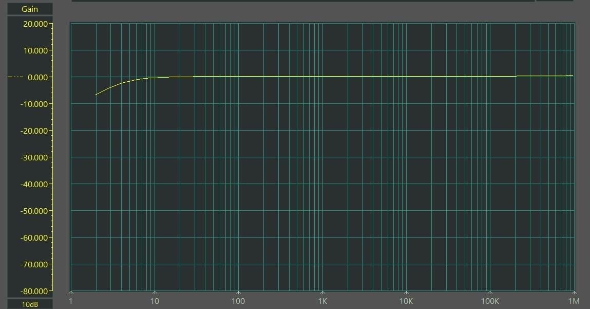
Figure 7. Frequency response with 1 V input on 1 V range [click image to enlarge].
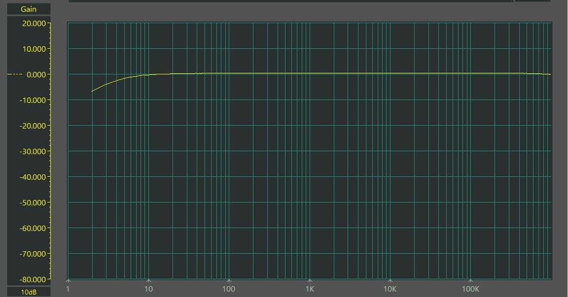
Figure 8. Frequency response with 100 mV input on 100 mV range [click image to enlarge].

Figure 9. Frequency response with 10 mV input on 10 mV range [click image to enlarge]

Figure 10. Frequency response with 1 mV input on 1 mV range [click image to enlarge].
The responses at 1.2 MHz are out of range of the sweeper, so they were measured with a signal generator. In this range, a small amount of noise on the trace is to be expected due to the small input and high gain. Figure 11 shows the response of the current meter at 100 mA.
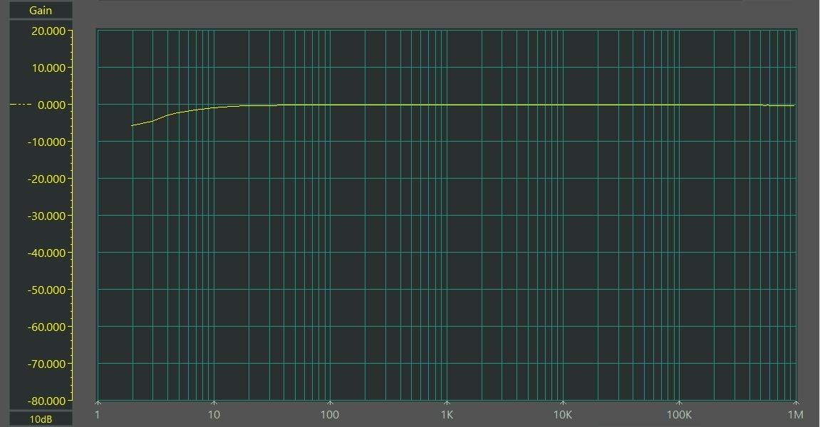
Figure 11. Response of the current meter at 100 mA [click image to enlarge].
Optional External Filters
External filters should have an input resistance of 10 kΩ or greater and an output resistance of 1 kΩ or less.
Construction Tips
To keep unwanted RF emissions out of the meter, a metal or conductive-plastic enclosure is needed. It may be necessary to put ferrite beads at all inputs and outputs as close to the connector as possible. A very low-value capacitor, such as 10 pF, might be required between the inputs of each op amp.
Possible Design Extensions
Several interesting extensions could be added to this design to provide additional features, including:
- An alternative, or selectable, true-RMS detector with 200 kHz bandwidth, using the reasonably-priced AD736 device
- A 22.4 Hz to 22.4 kHz standard unweighted audio noise filter
- An accurate A-weighting filter


This is a very interesting design for a wide range peak voltmeter, I like it.
However, the calculation of the power dissipation in some resistors is a little confusing to me; a 0,1Ω resistor for 10A is dissipating no more than 1W? The 8Ω resistor to calibrate the 1A range is dissipating only 0,125W? In both cases I should take a type that can dissipate 10W.
After all, every resistor has a temperature coefficient.