TSMC Certifies a Host of Top EDA Tools for New Process Nodes
With TSMC scaling down to 2 nm and lower, the semiconductor giant is working with Cadence, Siemens, and Synopsys to bring updated EDA tools to IC designers.
Taiwan Semiconductor Manufacturing Company (TSMC) is recognized as the world leader in semiconductor fabrication. Though the company is working with top EDA companies to certify their IC design tools for its 2 nm process technology, TSMC has already set its sights on 1.6 nm chips in the near future.

TSMC is constructing two new factories to support future 2nm process technology. Image (cropped) used courtesy of TSMC
Chip designers must have electronic design automation (EDA) tools to develop integrated circuits for these new nodes. To this end, some of the industry’s most prominent EDA companies, Synopsys, Cadence, and Siemens, each recently announced collaborations with TSMC to add support for TSMC’s latest nodes to their EDA tool suite.
Cadence: A Push for 3D ICs, Advanced Nodes, and Photonics
Cadence and TSMC recently announced a collaborative effort to optimize Cadence’s tool suite for TSMC’s 2-nm process technologies.
These optimizations cover a range of applications, from digital and analog design flows to semiconductor power integrity analysis. Cadence's Innovus Implementation System and Genus Synthesis Solution are now certified for TSMC's N2 design flows, and the Cadence Integrity 3D-IC platform now features enhanced capabilities for handling complex multi-chip designs using TSMC's 3DFabric technologies.

Cadence's Integrity 3D-IC platform. Image used courtesy of Cadence
The collaboration also extends to custom or analog tools optimized for TSMC's N2 Process Design Kit (PDK), including the Virtuoso Schematic Editor and the Virtuoso ADE Suite. These platforms support advanced circuit simulation and optimization necessary for high-performance and low-power semiconductor applications.
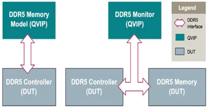
The partnership may advance photonic integrated circuit design, with new flows to support TSMC’s Compact Universal Photonic Engine (COUPE) technology. As part of this, the companies have introduced a comprehensive portfolio of IP cores optimized for TSMC’s N3 process technology, covering interfaces such as UCIe, DDR5, LPDDR5, GDDR6, PCIe 5.0/CXL2.0, and PCIe 6.0/CXL3.0.
Synopsys: AI-Driven Design Flows for N2
Synopsys is also teaming up with TSMC to optimize the fab's chip design processes using artificial intelligence and photonic integrated circuit (PIC) technologies.
TSMC is integrating the Synopsys.ai suite to facilitate efficient analog and digital design on its N3, N3P, and N2 process technologies. This includes the DSO.ai platform, which automates chip design and optimizes the tradeoff between power, performance, and area characteristics in advanced chip designs.
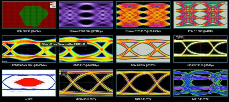
Synopsys IP on TSMC N3E. Image used courtesy of Synopsys
The collaboration aims to develop integrated radio frequency (RF) and photonic design flows as well. With modern processing paradigms like multi-die integrations demanding faster and more efficient inter-chip communication, developers are turning to photonic design to achieve higher data transmission rates with lower latency. Synopsys will use TSMC's COUPE technology in its Photonic IC design and 3DIC Compiler toolsets to streamline the design and manufacturing process of these photonic components.
Synopsys also announced improvements to its IP offerings for TSMC’s advanced nodes. This includes a broad array of Foundation and Interface IPs like UCIe, HBM4/3e, and PCIe 7.x/6.x.
Siemens: IC Verification Tools Certified for N2
Multiple Siemens EDA tools have successfully achieved certification with TSMC’s latest semiconductor processes, such as the advanced N2 process.
Key Siemens tools that received certification include the Calibre nmPlatform tool suite, which includes tools like Calibre nmDRC for design rule checking, Calibre nmLVS for layout vs. schematic verification, Calibre Pattern Matching, and Calibre PERC. The certification of these tools ensures they can support the TSMC N2 node, allowing for the design and production of smaller, more efficient, and powerful semiconductors.
Siemens' Calibre 3DSTACK. Image used courtesy of Siemens
Additionally, the Siemens Analog FastSPICE platform, known for its precision in verifying nanometer-scale analog, RF, mixed-signal, memory, and custom digital circuits, has been certified for TSMC’s N3P, N2, and N2P processes.
For 3D integration, Siemens’ Calibre 3DSTACK solution has been approved to support TSMC’s 3Dblox standard. This standard is a guideline for 3D IC designs that enables sophisticated thermal analysis as part of TSMC’s 3DFabric advanced packaging technologies. It allows designers to foresee and mitigate potential overheating issues in densely packed ICs, helping maintain performance and reliability in dense advanced nodes.
EDA for Next-Gen Nodes
Designers need EDA tools optimized for TSMC's new process nodes to fully leverage the technology's power. By collaborating with TSMC, companies like Cadence, Synopsys, and Siemens are directly integrating TSMC’s wealth of knowledge into their tool suite and providing IC designers with reliable tools to design the next generation of semiconductor products.