ISSCC 2024: Samsung Doubles DDR5 Capacity With Symmetric-Mosaic Architecture
In our final ISSCC spotlight, we explore Samsung's paper on a high-capacity, high-speed DDR5 memory that implements a monolithic-die-based 32-Gb DDR5 with 8 Gb/s/pin—all without leaving the 10 nm process.
The march of DDR5 performance continued at the recent IEEE International Solid-State Circuits Conference (ISSCC) with a paper by Samsung scientists.
Samsung aims to double DRAM capacity with its newly proposed architecture. Image (modified) used under Adobe Stock license
The paper, entitled “A 32-Gb 8.0-Gb/s/pin DDR5 SDRAM with a Symmetric-Mosaic Architecture in a 5th-Generation 10nm DRAM process,” covers the limitations of the currently used 16-Gb architecture and Samsung's proposed symmetric mosaic layout. In this article, we’ll summarize the key components of the architecture outlined in the paper.
From 16-Gb Die to Monolithic 32-Gb Die
Currently, the highest capacity DDR5 memories use a three-dimensional stacked (3DS) architecture based on a 16-Gb die and fabbed with a 10-nm process. The current mainstream end product is a 64-GB DDR5 DRAM module, with 128-GB modules increasing in demand.
The Samsung paper describes a monolithic 32-Gb high-density DDR5 die, still utilizing the 10-nm process. Samsung claims the 32-Gb die-based 3DS systems will improve performance, support memory up to 1 TB when used in eight die stacks, and achieve speeds of 8 Gb per second per pin.
The industry recognizes the need to move to a 32 Gb die. However, there are a number of obstacles. Nodes smaller than 10 nm for DRAM are not yet ready, so chipmakers must find ways to increase capacity without changing the fab process. Further, the current DRAM module form factor is too entrenched to increase package sizes without significantly increasing capacity or performance.
Mosaic Partitioning to Overcome Traditional DRAM Size Limits
The 32-Gb die will be an adaptation, not a new standard, and thus must accommodate conventional JDEC-dictated DDR5 form factor limits (10 mm x 11 mm maximum). Conventional methods for increasing capacity without decreasing process size involve adding DRAM cells within a bank or doubling the number of physical banks in a logical bank. This results in a rectangular memory footprint that exceeds the 10 mm x 11 mm package size bounding box in either the vertical or horizontal direction.
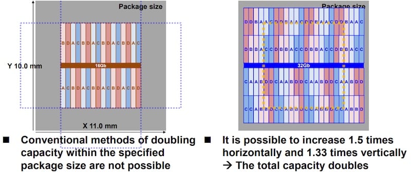
Comparison of die capacity increase with conventional methodology (left) and symmetric mosaic approach (right).
In the proposed architecture, each logical memory bank is broken into ⅓ and ⅔ partitions. These are interspaced as a symmetric mosaic of different partitions of the logical banks. This doubles DRAM capacity with only a 1.5 x horizontal and 1.33 x vertical area increase, which fits inside the bounding box.
Two partitions from different logical banks will share the same global I/O (GIO) signal line and sense amplifier. This sharing reduces the GIO line loading capacitance, boosting speeds and lowering power consumption. This physical layout keeps the I/O in the center, as is used in the 16-Gb die, shares the same pad structure, and utilizes a similar through-silicon via (TSV) structure to connect the 3DS layers.
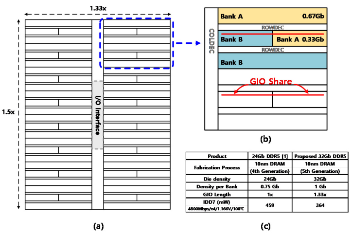
Symmetric mosaic architecture.
The mosaic interleaving and sharing of the GIO line takes advantage of the precise timing of the guaranteed read-to-read and write-to-write timing specification (tCCD_L). The physical memory banks are divided and accessed as logical banks, with the tCCD_L characteristics used to dictate the timing.
Increasing Speed and Decreasing Interference
Keeping the data accurate at such high speeds requires extra logic for what is called decision feedback equalization (DFE). High speed digital is not the simple “on/off” voltage transition as is seen with lower speeds. Signals are rounded, interfered with, and often act more analog than digital. Signal line capacitance and resistance essentially create filters with R/C time constants that distort and impede the information-carrying signal (the symbol). The effects of one symbol can bleed into the next, or reflections from the receiving component can distort the symbol, causing inter-symbol interference (ISI), which must be mitigated to prevent invalid data.
Samsung’s proposed architecture adds to conventional DFE circuits with a four-tap system—an alternative to conventional two-tap DFE. In a DFE circuit, the taps are fed back to the input and summed. The four-tap directly feeds tap one back to minimize feedback delay. The second, third, and fourth taps use current model logic (CML) summation to further enhance the symbol accuracy.
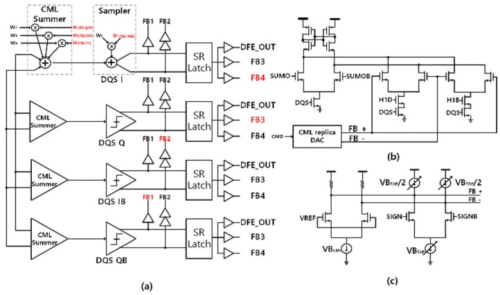
(a) Four-tap DFE. (b) Tap one directly feeds the sampler. (c) Taps two through four into the CML circuit.
The DFE operates along with automatic-offset-voltage-calibration circuitry in the DQ buffers. The calibration circuit compensates for offset by using four paths for four phases of the operation and calibrates based on a direct majority voting of the four path outputs. The result is the ability to reliably operate at 8 Gb/s or faster.
Chip ID Pre-Decode
With double the RAM cells per die, power consumption becomes even more critical than with a 16-Gb die. Because these chips will largely be installed in 3D-stacked configurations, chipmakers must improve the process of targeting inefficient chips.
A “rank” is a logically combined set of physical banks that carry the same data word width as the on-die data bus. It can be formed within a physical die or across multiple dies in a 3D-stacked die system. For example, the upper left quadrant of each of eight-stacked dies could be combined into and addressed as one 8-bit logical rank.
In a standard configuration, a command comes into the command bus with a chip ID (CID). All ranks then perform decoding to see if they are the intended target. Once the decode is done, only the intended rank follows through. Having all ranks perform the decode operation wastes a significant amount of power.
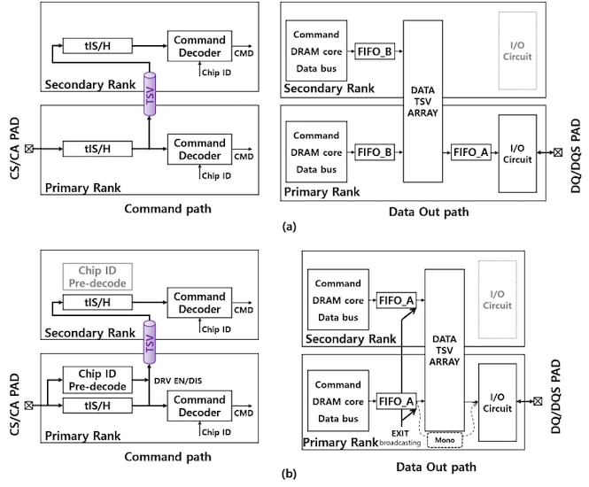
(a) Traditional CID decode stack and (b) Samsung's proposed pre-decode system.
This proposed architecture comes with a chip-ID-pre-decode in each rank. With such functionality, the primary rank has pre-decode circuitry before the TSV. It only sends the CID to the next rank if it is not the intended target. Essentially, each rank in the stack will stop the CID when it is the intended target. If the last rank in the stack is the intended target, no power is saved, but for all ranks below the top, a proportional amount of power is saved.
Progress Within Today’s Form Factor
Samsung’s proposed architecture significantly increases DRAM capacity without changing the overall form factor or decreasing chip etch geometries. By using a more efficient, though non-traditional, organization structure, more can be fit into the same area without standards or fab changes. The proposed architecture employs logical ranks, timing idiosyncrasies, and resource sharing to increase capacity, reduce power consumption, and increase maximum speed.
By Samsung’s measurements, a 32-Gb-based 0.5 TB DIMM consumes 30% less power than a 16-Gb-based part, making it a useful drop-in for data centers and other capacity- and power-hungry computing applications.
All technical images used courtesy of Samsung and ISSCC.