AMD Launches Embedded+ Architecture Blending Ryzen and Versal
Unveiled today, the new architecture hopes to facilitate sensor integration, offloaded processing, and faster times to market.
The demands of modern-day processing are following a couple of common trends. One trend is the increasing need for sensor integration so that processing can be done on a variety of different sensor inputs at once.
To complement this, the processing has moved to the edge, where computation and AI inference can happen closer to the sensors themselves. The real challenge, however, lies in achieving all of this in a small enough footprint and low enough power consumption for a battery-powered IoT device

AMD’s Embedded+ offering
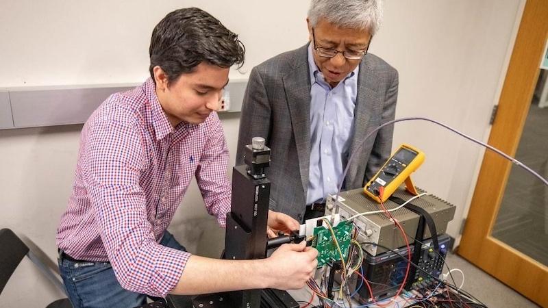
To bring the best of all worlds to engineers while simplifying the design process, today AMD has launched its new Embedded+ architecture. But what’s new with Embedded+, and how does AMD think it will revolutionize the industry? All About Circuits had the chance to talk with Chetan Khona, AMD’s Senior Director for Industrial, Vision, Healthcare, and Sciences, to answer these questions directly.
Embedded+ Architecture: Sensors and Processing
Embedded+ is a new SoC architecture from AMD that combines AMD Ryzen Embedded processor technology with Versal SoCs on a single board. Khona explained the fundamental goals of the new architecture. “When designing the Embedded+, the three key elements of the architecture that we focused on were that it needed to be sensor friendly, support offloaded processing, and help customers decrease time to market,” he says.
With respect to sensing, the Embedded+ architecture is designed to allow for the seamless integration and management of multiple sensor inputs, which is crucial for applications in IoT, industrial automation, and healthcare devices.
To this end, the architecture provides direct support for a myriad of different sensor inputs, including image sensors, LiDAR and radar, IMUs, and more. This is facilitated through a combination of PC and network connectivity interfaces, such as Ethernet, USB, and HDMI as well as dedicated “adaptive I/O” for real-time sensor input and industrial networking.

Embedded+ based motherboard interfaces
Offloaded processing is another focus, which enables the delegation of compute-intensive tasks to specialized processing units within the system. This approach frees up the main processor to handle other tasks, improving overall system performance and responsiveness.
To do this, the Embedded+ Architecture builds on the Ryzen Embedded R-Series SoCs. This SoC has 4C/8T Zen+ x86 CPU cores along with 8 AMD Radeon graphics compute units. These R-Series SoCs are then coupled via PCI Express with a Vesal AI Edge SoC, featuring Dual-Core Arm Cortex-A72 application processors, Arm Cortex-R5F real-time processors, and dedicated AI and DSP engines. Finally, the system is completed by dedicated programmable logic meant for sensor fusion and real-time control functions.
Summing up the versatility of the architecture, Khona explains how it meets a variety of needs.
“If you need things like low latency deterministic networking and sensor interfacing, Embedded+ offers the expansion connector, the programmable I/O, FPGA fabric. If you need real-time control, it offers the Arm subsystem and also the FPGA fabric. And if you need AI inferencing, the Versal AI Edge family offers AI engines as part of their architecture, and that's a part of Embedded+ as well."
Embedded+ Architecture: Time to Market
The final focus of Embedded+ is to help designers bring their designs to market faster. One way this is achieved is through the use of a common software infrastructure that simplifies development and integration within the Embedded+ architecture.
The use of a unified software infrastructure means that developers can rely on a consistent set of tools and APIs across different projects, which not only accelerates the development cycle but also ensures higher reliability and compatibility across the board. This approach minimizes the need for custom development and troubleshooting, which are often time-consuming and resource-intensive.

Embedded+ offers a unified software infrastructure.
Moreover, by leveraging AMD's ODM (Original Design Manufacturer) ecosystem, developers gain access to a range of pre-validated solutions. These solutions have already undergone rigorous testing and qualification, ensuring that they meet the necessary standards and performance criteria.
This pre-validation process significantly reduces the time and effort required for system qualification and testing, allowing developers to focus on application-specific functionalities rather than the underlying hardware and software integration.
The combination of a common software infrastructure and the support of an ODM ecosystem effectively reduces the barriers to entry for developing sophisticated embedded systems. It enables faster deployment by simplifying the development process, from initial design to final product, thus providing a competitive edge in the fast-paced market of embedded technologies.
AMD reports that the first ODM board is the Sapphire Edge+ VPR-4616-MB, a low-power Mini-ITX form factor motherboard from Sapphire Technology.
Available Soon
As more devices demand a combination of low power, sensor integration, and edge computing, AMD is answering the call with their new Embedded+ architecture. Built on the tenets of being sensor-friendly, supporting offloaded processing, and reducing time to market, the new architecture hopes to facilitate the development of next-generation edge devices for applications ranging from medical to automotive.
All images used courtesy of AMD