Facebook
 Google
 GitHub
 Linkedin
4 New Memory ICs Scale From AI Accelerators to Industrial Sensors
New HBM, UFS, NAND, and EEPROM devices span the storage stack.
Regardless of use case, intelligent products rely on memory. Whether that’s AI workloads in hyperscale data centers or industrial sensors making decisions at the edge, engineers need dense, fast, and reliable memory solutions for their deployments.

Recently, GigaDevice, Samsung, Kioxia, and SK Hynix each announced new memory products that span the full stack of use cases that rely on memory.
GigaDevice Branches Into I2C EEPROM
Industrial and networking equipment that stores configuration data needs memory that survives frequent rewrites and years of continuous operation without corrupting the data it holds. To meet this need, GigaDevice launched the GD24CL series, an I2C EEPROM line that marks the company's first entry into the EEPROM market and expands its non-volatile memory portfolio beyond flash.
For industrial applications, the series offers endurance of up to four million program-and-erase cycles—four times the industry standard cited by GigaDevice—along with data retention rated at up to 100 years. To further bolster memory, the company built in a hardware-level error-correction code and added a Write Protect pin, along with a write-lockable Security Page, that together prevent erroneous or malicious overwrites of stored data.

GigaDevice BD24CL Series I²C EEPROM. Image used courtesy of GigaDevice
For versatility, the series also supports three I²C clock frequencies (100 kHz, 400 kHz, and 1 MHz), covering everything from low-speed sensors to high-speed industrial control systems. The GD24CL256B, a 256-Kb device, is the first product in the series with samples available, with GigaDevice planning to launch 128-Kb and 512-Kb variants in the first half of next year, eventually spanning capacities from 32 Kb to 1 Mb.
Samsung Rolls Out UFS 5.0
As generative AI models move from the cloud to smartphones and wearables, on-device storage must keep up with processors that now run large language models locally. To that end, Samsung developed a new Universal Flash Storage (UFS) 5.0 solution with a sequential read speed of up to 10.8 GB/s and a sequential write speed of up to 9.5 GB/s, more than double the throughput of the previous UFS 4.1 standard. The company attributes the gain to the integration of the latest UFS interface standard from JEDEC.
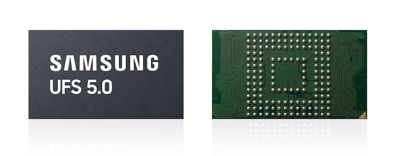
Samsung UFS 5.0 solution. Image used courtesy of Samsung
However, faster storage alone is not enough. Samsung also improved power efficiency by more than 40% over UFS 4.1 by using clock gating and multi-voltage techniques that reduce the energy required to transfer the same amount of data. The company packaged the storage into a 7.5 mm x 13 mm x 0.9 mm module, 16.7% smaller than its predecessor, freeing board space for compact form factors like XR headsets.
The company plans to begin mass production in the fourth quarter of this year, in capacities up to 1 TB.
Kioxia Intros Next Generation of BiCS Flash
Enterprise and data center SSDs supporting AI storage need NAND flash that packs more bits per die area without increasing the rack power budget. For these customers, Kioxia built new 1-Tb triple-level-cell (TLC) memory devices on its 10th-generation BiCS FLASH 3D flash memory technology. The company has begun shipping samples mainly for enterprise and data center SSDs.
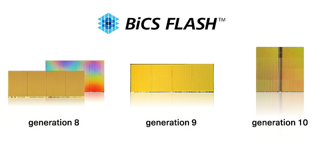
Kioxia BiCS FLASH 3D flash memory generations 8 to 10. Image used courtesy of Kioxia
The new generation stacks 332 layers. Combined with improved lateral density, that stacking raises bit density by 59% over the prior generation. Kioxia carried forward CMOS-directly-Bonded-to-Array (CBA) and On-Pitch Select Gate Drain (OPS) technologies from its 8th-generation devices, helping the 10th generation reach a NAND interface speed of 4.8 Gb/s, a 33% improvement over the 8th generation. The company also claims that write and read power efficiency improved by 18% and 30%, respectively.
SK Hynix Stacks 12 Layers High With HBM4E
While stacking additional DRAM dies onto a single HBM package increases capacity and bandwidth, each added layer also increases the thermal and mechanical stress. SK Hynix solved this problem with its next-generation HBM4E using a 12-layer, or 12-Hi, stack architecture to reach 48 GB of capacity in that footprint.
The company says the 12-layer stack was made possible by its Advanced MR-MUF packaging process, which injects liquid protective material between dies during stacking and reportedly reduces heat resistance by 17% compared with the previous HBM4 generation. SK Hynix also claims that the reduction helps the stack maintain stable operation as engineers add layers for large-scale AI computing systems.
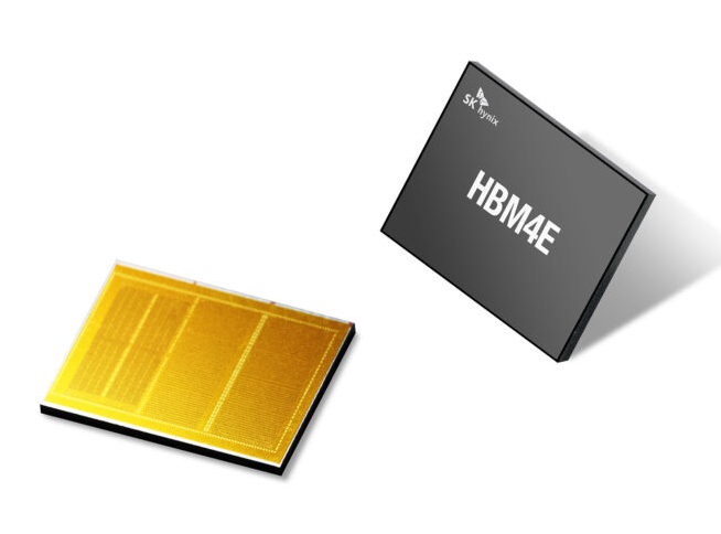
SK Hynix HBM4E DRAM. Image used courtesy of SK Hynix
The HBM4E reaches a maximum data processing speed of 16 Gbps per pin and, according to the company, improves power efficiency by more than 20% over prior models, lowering data transfer latency for AI training and inference workloads on data center accelerators. The company just started shipping samples of its next-generation HBM4E to major customers.
Memory Advances Span the Full AI Storage Stack
Regardless of the application, memory remains a high priority in next-generation designs, and suppliers are clearly aware. Together, these four announcements show how different memory leaders are optimizing solutions at every layer of the AI storage stack.