Resolving the Signal Part 8: How Voltage Reference Noise Affects Delta Sigma ADCs
Part 8 of the Resolving the Signal series dives further into how different noise sources impact precision delta-sigma ADCs by focusing on reference noise and ADC noise, and how gain affects reference noise.
Part 8 of the Resolving the Signal series dives further into how different noise sources impact precision delta-sigma ADCs by focusing on reference noise and ADC noise, and how gain affects reference noise.
Imagine that you need to design a high-resolution sensor measurement system such as a precision temperature sensing unit to control an industrial oven. To accomplish this, you install a thermocouple in the oven to measure the temperature, attach the thermocouple leads to the measurement system, and the analog-to-digital converter (ADC) outputs a digital code. How do you determine the actual temperature to which that code corresponds?
In analog circuit design, you use a voltage reference as the baseline against which analog measurements are made. In the context of this example, the nominal voltage of the reference determines the resulting output code, which correlates to a specific temperature. If you changed the reference voltage, the output code would scale as well, while the measured temperature would remain the same.
Since the output code is directly related to the value of the reference voltage, a noisy or inaccurate voltage reference yields measurements that are similarly unreliable. Therefore, for high-resolution systems, choosing an appropriate voltage reference is equally as important as choosing a precision ADC.
To further understand how different noise sources impact precision delta-sigma ADCs, I’ll discuss the following topics as they relate to voltage reference noise in this installment of the “Resolving the Signal” article series:
- Reference noise and ADC noise
- How gain affects reference noise
In part 9, I’ll take the observations from part 8 and define several ways to reduce reference noise. I’ll also examine how reference noise affects low- and high-resolution ADCs.
Reference Noise and ADC Noise
In part 2 of this series, I discussed two different types of measurements used to characterize ADC noise: sine wave-input and input-short. Sine wave-input, as its name implies, inputs a sine wave with a specific amplitude and frequency to characterize how the ADC quantizes this signal. Conversely, the input-short method determines ADC performance at DC by shorting the device’s inputs and measuring the slight variations in the output code as a result of thermal noise. Figure 1 illustrates these types of noise measurements.
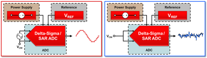
Figure 1. Sine-wave-input test setup (left); input-short test setup (right)
The ADC’s output code is proportional to the ADC input signal amplitude (VIN) divided by the ADC’s reference voltage (VREF), as expressed by Equation 1:
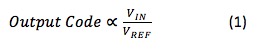
When we use a nonzero input signal to characterize an ADC – as is the case with the sine-wave-input method – the resulting output code includes some reference noise. While the intent is to characterize only the ADC noise, this reference noise invariably becomes part of the noise parameters reported in the ADC’s datasheet, including signal-to-noise ratio (SNR) and signal-to-noise ratio and distortion (SINAD).
Therefore, using a system similar to the ADC’s testing setup allows you to achieve ADC noise performance comparable to what is reported in the datasheet for devices characterized by the sine-wave-input method.
Comparatively, the input-short method uses a 0V input signal to measure the fluctuations in the ADC output code when no signal is present. In this case, no reference noise is seen at the output because the ratio in Equation 1 always equals 0. The input-short method defines an ADC’s absolute resolution limit, since you cannot expect to reliably measure an input smaller than the ADC’s inherent noise. As a result of the shorted inputs, data-sheet noise parameters such as input-referred noise and effective resolution do not include the effects of reference noise. If you want to measure a nonzero input signal with this type of ADC, you should expect the previously unseen voltage reference noise to increase the total noise seen at the output beyond what is stated in the ADC’s data sheet.
To determine how much noise the voltage reference adds, Figure 2 shows the relationship between ADC noise, reference noise and combined noise as a function of how much of the full-scale range (FSR) is used (percent utilization). Figure 2, along with the subsequent discussion, is applicable to cases where the ADC noise is less than the reference noise (NADC < NREF). If the opposite were true (NADC > NREF), the lower-noise voltage reference would offer little to no benefit due to comparatively higher ADC noise.
.png)
Figure 2. ADC noise (blue bar chart), reference noise (red bar chart) and combined ADC plus reference noise (green line) as a function of positive FSR utilization
Figure 2 has three important points:
Point A
This point is the total noise when the input voltage is 0V. Since Point A uses the same conditions that define the input-short noise measurement test, you can read it directly from the ADC’s data sheet.
Point B
This is the total noise when the input voltage is equal to the reference voltage – that is, a full-scale reading. In general, take the root sum of squares (RSS) of the reference noise and the ADC noise to determine Point B. However, when the reference noise is much larger than the ADC noise – as is the case in Figure 2 – Point B can be approximated as just the reference noise. Either way, you generally cannot read the value of the voltage reference noise directly from the datasheet, since it depends on several factors including the voltage reference’s noise characteristics. Figure 3 shows the output noise spectral density for the Texas Instruments REF6025, a 2.5V precision voltage reference.
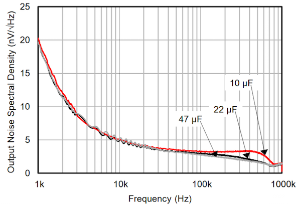
Figure 3. Output noise spectral density plot for the REF6025
In Figure 3, note the significant increase in noise density at low frequencies (1/f noise) compared to the relatively flat noise density at higher frequencies (broadband noise). Like several of the amplifiers analyzed in part 7 of this series, reference noise performance is not necessarily constant over frequency.
Fortunately, you can use the same methods to calculate reference noise that you use to calculate amplifier noise, including direct integration or simplified formulas. You will also need to calculate the system’s effective noise bandwidth (ENBW) to use these methods, as ENBW provides a cutoff frequency for the reference noise entering the system.
Point C
This point is any generic noise value between the extremes of Points A and B. You can calculate Point C using Equation 2:
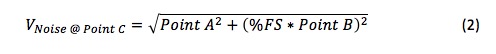
In Equation 2, Point B scales according to the percent utilization of the FSR. In general, you can use Equation 2 to determine the total noise at any point on the plot in Figure 2, including Points A and B.
One important result of Equation 2 is that given the condition that NADC < NREF, there exists a point at which reference noise dominates regardless of percent utilization. At this point, increasing your signal amplitude offers no noise performance benefit, which contradicts the common belief that gaining up the input signal always reduces noise.
Instead, you need to balance increasing gain and FSR utilization to ensure that you meet the system noise requirements. Let’s examine the relationship between gain and reference noise with an example.
How Gain Affects Reference Noise
For this example, let’s continue using the REF6025 shown in Figure 3 and pair it with the ADS1261, a 24-bit delta-sigma ADC. This device offers low noise and an integrated programmable gain amplifier (PGA), both of which will make the reference-noise-versus-gain relationship more apparent. Despite these choices, you can apply this analysis to any combination of ADCs and voltage references. Figure 4 shows the system setup for this example.
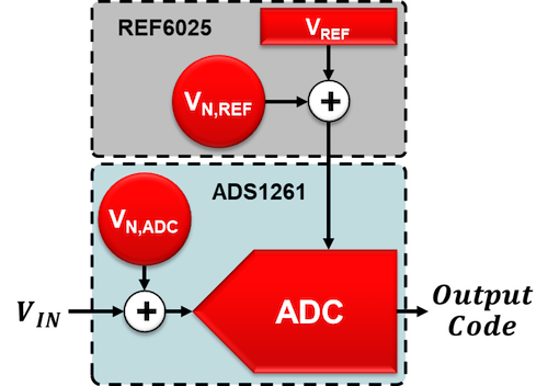
Figure 4. System setup using the ADS1261 and REF6025
Similar to amplifier noise analysis in part 6 of this series, you can separate the components in Figure 4 into “noiseless” devices preceded by a voltage source that is equivalent to each component’s noise. The ADC noise (VN,ADC) can be read directly from the ADS1261’s data sheet, while you must calculate the voltage reference noise (VN,REF) using the REF6025 data sheet as well as the system ENBW. Fortunately, you can use the approximation methods I detailed in part 5 of this series to determine the system ENBW. In this case, the ENBW is 13Hz using a 60 samples-per-second (SPS) output data rate (ODR) and the low-latency filter of the ADS1261. This yields approximately 1.2µVRMS of noise using the REF6025.
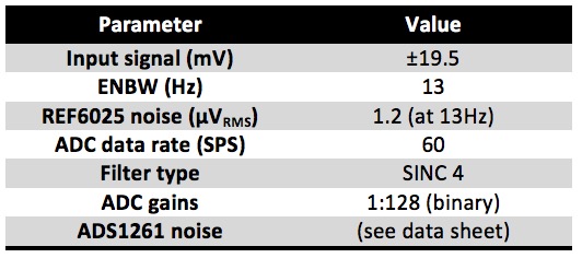
Finally, you need to choose an input signal that allows you to use all available ADC gain options. Using the ADS1261’s maximum gain of 128V/V enables a maximum differential input voltage of ±19.5mV using a 2.5V reference voltage. Table 1 summarizes the system specifications.
Table 1. System specifications for the ADS1261-plus-REF6025 example
You can now plot the noise of each component as a function of the ADS1261 PGA’s gain to see how gain affects ADC and reference noise. You can also calculate the system’s effective resolution at each step to understand how the introduction of reference noise affects the system’s dynamic range. Note that “effective resolution” in this context is calculated using a 19.5mV signal and not the maximum possible FSR at each gain setting, as is common in ADC data sheets. Figure 5 shows the plot for the ADS1261.
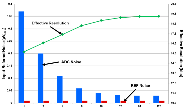
Figure 5. ADS1261 noise, reference noise and effective resolution as function of gain
Figure 5 shows that the reference noise is almost negligible compared to the ADC noise even when using 100% of the positive full-scale range. Changing the gain therefore had no effect on how much reference noise was passed into the system due to the very small input voltage, but did reduce the total noise by reducing the ADC noise (as expected).
Interestingly, both Figures 2 and 5 have a useful FSR utilization limit (as was the case with the amplifier noise analysis). Increasing the input signal beyond this point offers no benefit from a system noise perspective. In Figure 2, this occurred at a 40% utilization factor. In Figure 5, this limit began at approximately a gain of 32 V/V as the effective resolution curve begins to flatten.
(These limits are specific to this input voltage, noise bandwidth, ADC and reference combination. Different combinations change this system limitation, making it essential to calculate where this point is in any system to avoid degrading noise performance.)
Moreover, Figures 2 and 5 demonstrate the importance of matching your ADC noise to your voltage reference noise (as they relate to your circuit parameters). If your input signals are small and cannot be changed, gaining up your input signal reduces your ADC noise and therefore the total system noise. You might also be able to use a noisier reference as a result, since very little reference noise will actually be passed into the system.
Comparatively, if your input signals are greater than mid-scale you can expect the reference noise to dominate. In these cases, you should always make sure the ADC noise and reference noise are comparable. Otherwise you will be paying for voltage reference performance that you cannot actually use. Fortunately, there are multiple ways to reduce the effects of reference noise and maintain precision systems. Read part 9 to learn more.
Key Takeaways
Here is a summary of important points to help better understand how voltage reference noise affects delta-sigma ADCs:
- The system noise contribution from the reference voltage scales with FSR utilization.
- Reference noise can have 1/f and broadband regions similar to amplifiers.
- Reference noise in a system results in a useful FSR utilization limit, after which noise performance cannot be improved further through signal gain.
- Try to match the reference source’s noise amplitude to the ADC’s noise performance to avoid degrading resolution with nonzero input signals.
Industry Articles are a form of content that allows industry partners to share useful news, messages, and technology with All About Circuits readers in a way editorial content is not well suited to. All Industry Articles are subject to strict editorial guidelines with the intention of offering readers useful news, technical expertise, or stories. The viewpoints and opinions expressed in Industry Articles are those of the partner and not necessarily those of All About Circuits or its writers.