
Performing Design for Manufacturing Checks on Gerber Files
Avoid mistakes when exporting PCB files from your EDA tools into the Gerber format by understanding the translation process and using DFM tools.
Ucamco states in its Gerber Layer Format Specification:
Any problems in PCB fabrication data transfer are not due to limitations in the Gerber format but are due to poor practices and poor implementations.
So, you may be thinking, “If my PCB layout looks fine in my EDA software, then it should be fine when it is manufactured, right?” In an ideal world, yes.
However, each EDA tool builds with and organizes designs in its own language. That tool-specific language must then be translated into the language of Gerber files. There can be many problems that occur during that translation process. Many known problems have been dealt with over the years, but you can never be sure. Avoiding these problems may require you to have some background knowledge of the Gerber files and their use.
This is the final installment of our three-part article series in which we:
- Explain the Gerber file format, file names, and standards revisions.
- Help you understand the Gerber layers used for PCB and stencil manufacturing.
- Explain the importance of Design for Manufacturing (DFM) checks and introduce free resources.
Through this series, we will demonstrate why it is important to check your Gerber file before sending it to the PCB manufacturer, help you identify and avoid common problems, and describe Gerber file checks that you should be performing.
If you read part 1 of this article series, you have a background on the Gerber format and file names. In part 2, we provided a layer-by-layer explanation of the name, abbreviation, and purpose of each layer in a basic PCB. Now, here in part 3, we will demonstrate the importance of DFM checks prior to manufacturing and help you avoid some common mistakes.
Translation to the Gerber Format
Many problems are simply caused by incorrectly configured settings in your EDA tool. Likely, you will have noticed that there are many options to choose from and boxes to check when you come to exporting Gerber files, and there are numerous guides online for each EDA tool.
It is very easy for inexperienced users to select the wrong option or use the wrong tool to draw something, and since manufacturers' requirements may differ slightly, getting precisely what you want can be a long and tiring process. It is difficult to summarize all the potential problems that can occur since there are so many different EDA software and different versions. You won’t know unless you encounter the problem for yourself or manage to spot it in a Gerber Viewer. But let’s take a look at a few examples.
Gerber Export Error Example 1 - Different Fonts
Compare the three text font options (vector, proportional, and fixed) from Autodesk Eagle, as shown in Figure 1, with the resulting exported Gerber text shown in Figure 2. We are not sure why anyone would use fixed text in Eagle since it doesn’t display well, but we have included it anyway.
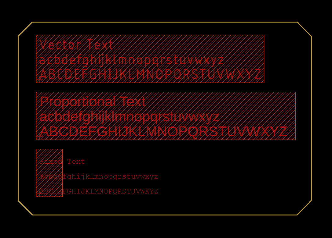
Figure 1. Three font options for text from Autodesk Eagle’s PCB editor
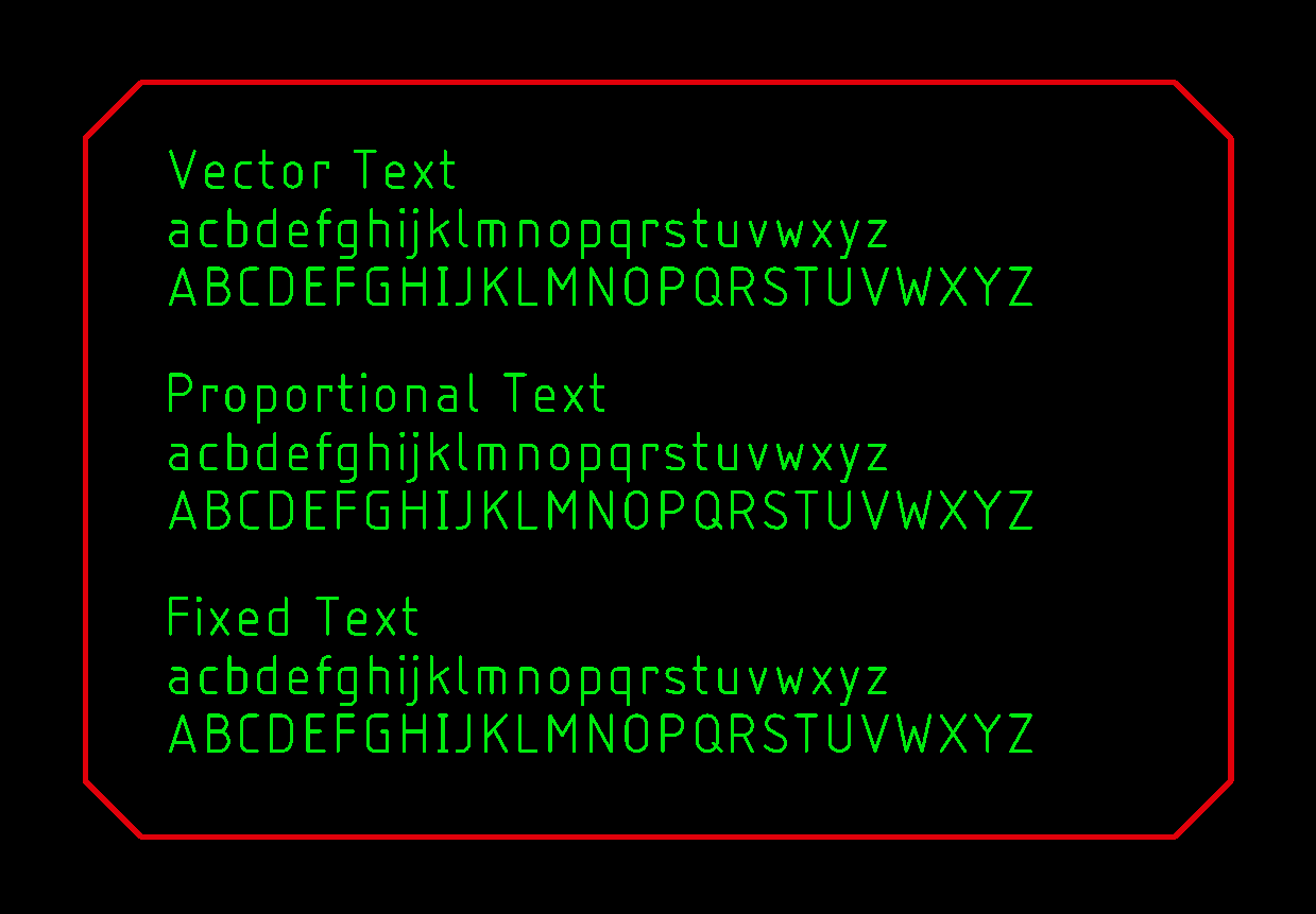
Figure 2. The Gerber text after exporting from Eagle.
In Eagle, proportional text and fixed text are converted to vector text when exported to Gerber files. The result is that the proportional text is slightly smaller. Though this size change for text layers is not likely to affect the functionality of the circuit board, this is a visual example of how what you see in the design data is not necessarily what you get.
Autodesk’s solution to this problem is to add an option to change the default text in the PCB editor to vector text, but this is hidden away in the settings, and newcomers won’t have a clue why the option exists.
Gerber Export Error Example 2 - Mechanical Elements on All Layers
Some EDA tools, such as Altium Designer and KiCad, have the option to plot the contents of a layer onto all other layers, as noted in the section highlighted by the blue box in Figure 3. This can be helpful for copying the board outline to other layers, for example. However, users must be careful not to accidentally check the wrong layer, or you could introduce short circuits and completely ruin the boards. Since this only affects Gerber data, such a problem could go unnoticed if the Gerber files are not checked.
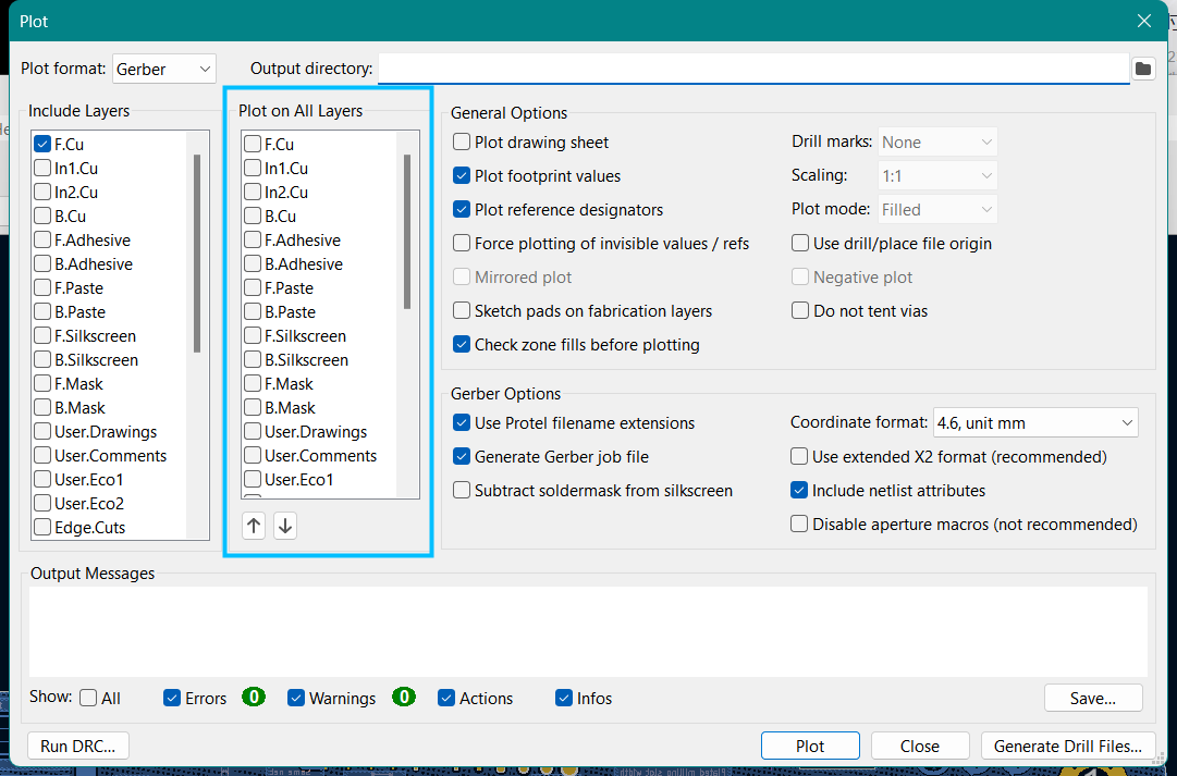
Figure 3. Export settings for creating the copper layer (click to enlarge).
But what happens if you have accidentally selected to plot your top silkscreen on all layers? As shown in Figure 4, you can get text merged with your desired copper circuit traces.
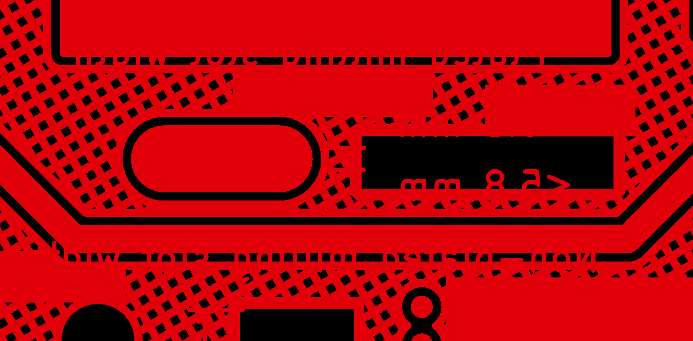
Figure 4. Silkscreen data was incorrectly exported onto the copper layer creating shorts.
When this gets manufactured, that undesired text will create short circuits where it overlaps adjacent traces.
Understanding Gerber Files So You Can Talk With Your PCB Manufacturer
In addition to avoiding the potential problems demonstrated above, there are many other benefits to having the tools and know-how to analyze Gerber files. In the following subsections, we will look at a few other benefits of understanding Gerber files.
The main reason you should put the time into familiarizing yourself with Gerber files is to better communicate with your fab house. Fab houses that perform Design for Manufacture reviews will check the Gerber files for errors such as shorts, missing pads, or areas that look unusual or don’t make sense.
They review the Gerber files since this is what they will use for fabrication. If they find errors and you have no idea what they are talking about, then good luck trying to fix the problem!
Just as the Gerber format has become the standard for PCB production data, Gerber files have become the universal language for communicating PCB design. Gerbers are multi-lingual; they can be understood by Japanese, Chinese, European, and American manufacturers alike, unlike localized EDA tools. Being able to read them helps your fab house work with you to resolve potential problems in your design.
No one expects designers to be manufacturing experts, but a basic understanding of manufacturing and the manufacturer’s perspective can go a long way to improving efficiency and improving current and future designs.
Confusing Gerber Data Example - Altium Mechanical Layers
Altium Designer provides a high level of flexibility and support for advanced features. That’s great if you need to give additional information to your assembly house or need ways to communicate advanced requests like selective surface finishes, carbon pads, etc. But often, designers export more than they need and not as intended, which causes confusion with the board manufacturer.
By trying to understand the design from the Gerber files, you can see where misunderstandings could occur. How does my manufacturer know how to produce my boards from just these files? Altium may export over 10 different Gerber files with the extension GM, some of which do not contain any useful information. Your manufacturer has to sift through all these layers to find any information pertaining to the board outline and then put them together.
Altium also encourages separating information, such as v-scores and routing. In addition, the outlines of the boards and panel are put into different mechanical layers. Most manufacturers prefer these be placed together to prevent details being missed which makes mistakes easier to detect.
For example, compare Figures 5 and 6. The green lines at the left of Figure 5 define part of the panel outline. Ar right, the outline in yellow is the keep-out layer (GKO). The keep-out layer is typically used to mark the clearance between the board edge and any components and copper traces; however, some designers use it to place the board outline.
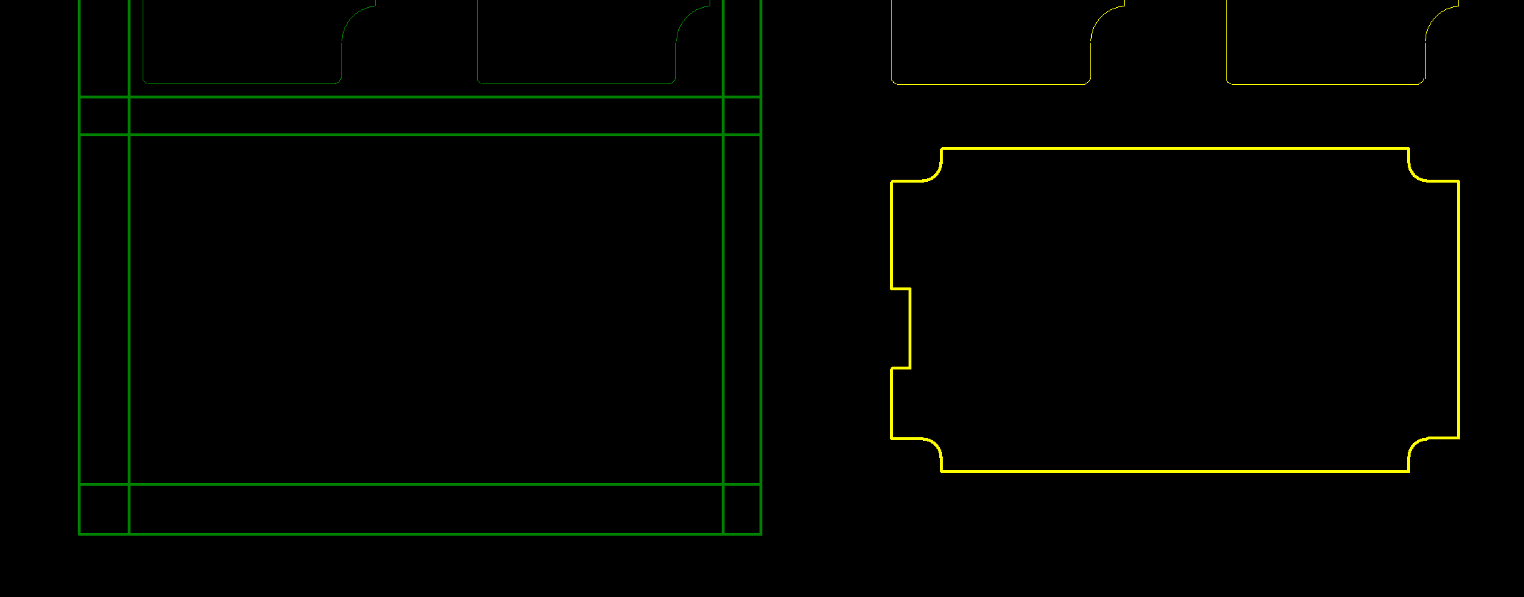
Figure 5. (left) panel outline in green and (righ) keep-out layer in yellow.
In Figure 6, the two layers are superimposed over each other. Comparing these images, can you work out how to produce this PCB? Is the keep-out layer the board outline, or is it the rectangle in the panel outline? The panel outline contains the board outline of some other boards above it, but not the large rectangular one.
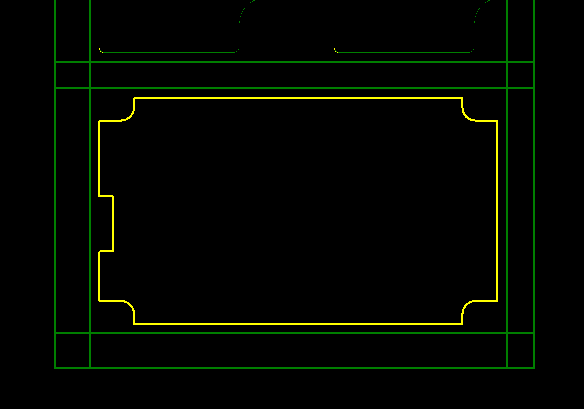
Figure 6. Overlay of the panel outline (green) and keep-out layers.
Only by adding the silkscreen layer, as shown in Figure 7, can we see the tabs connecting the board to the panel and the designer’s intention. The boards are supposed to be routed out following the keep-out layer, leaving tabs with stamp holes to hold it to the panel.
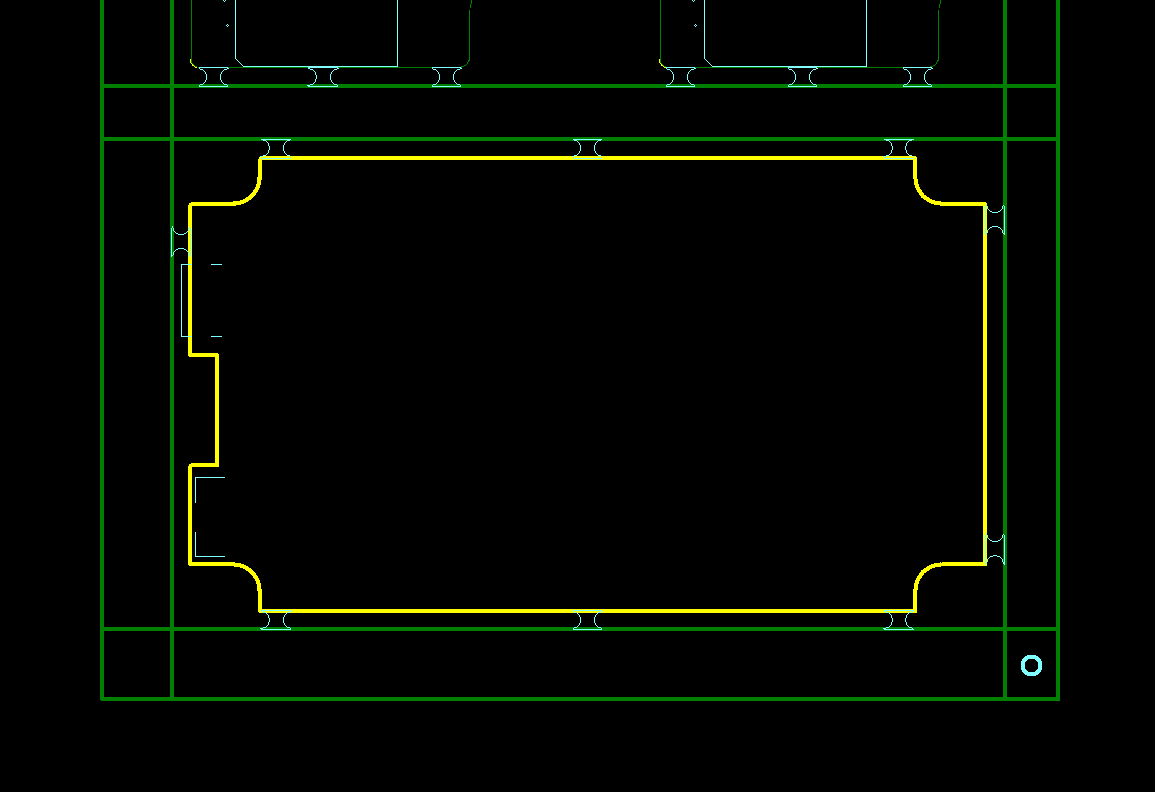
Figure 7. Adding the silkscreen layer to the panel and keep-out layers.
There are two mistakes here:
- The panel outline is missing the yellow routed outline.
- The tabs should be in the panel outline, not the silkscreen layer.
If the manufacturer only followed the green panel outline, they would have produced rectangular boards separated by v-cuts.
This kind of problem is difficult to catch in a Design Rule Check (DRC) or Design for Manufacturing (DFM) check. It can only be understood by looking at the Gerber files.
Understanding Gerber Files So You Can Check the CAM Production Files
When Gerber files are sent to manufacturers, a computer-aided manufacturing (CAM) engineer modifies the files slightly to convert them into instructions used by the various machines and manufacturing processes. At the same time, they will add production numbers, UL markings, and other manufacturing data. They will also modify traces for impedance matching and panelize the data if requested.
Some manufacturers will provide you the option to check post-edited Gerber files before going into production. Checking these production (working) Gerbers is the best way to accurately predict how your boards will be produced. If you sent special instructions or you are not sure you indicated a feature in the Gerber files correctly, double-checking the production files Gerber files is recommended.
For example, panel design and special requirements can be difficult to communicate clearly in words. With one glance, you can review the panelized data and confirm if there are any issues.
Another reason to check the production files is to look for any major mistakes made by the CAM engineer. Producing production files is largely manual work, and errors can occur! Since the designer should be the most familiar with the layout, they can help spot any obvious mistakes, such as an accidentally deleted copper pour or silkscreen marking. If it is important your boards are produced precisely the way you want, checking production Gerbers is a must.
Say, for example, you receive your boards and discover a short. Off the bat, you may be tempted to blame the manufacturer for poor quality control. But nowadays, automated optical inspection (AOI) and in-circuit testing (ICT) are implemented in almost all large factories. These can catch 99%+ of shorts caused during manufacture. If a manufacturing short occurs, it will only affect one or two boards.
If all of the boards are affected, this is a strong indicator that the problem lies with the production data. If you have done your DRC checks, then the design file should be free of shorts. So your first step should be to look at the original and production Gerber files. Maybe they were exported incorrectly, or maybe the CAM engineer moved something. The factory follows the files modified by the CAM engineer, not the original data, so if the short is present in the production Gerbers, it will not be picked up by AOI or ICT.
Using DFM Checks To Improve Your PCBs
You may be thinking, “Hey, it’s my manufacturer’s job to report problems with my files.” While DFM review has become a service included by default in most fabs, the level of detail will vary considerably across manufacturers and even across engineers from the same company, perhaps not to your liking.
Because DFM review is performed just before manufacture, any problems found will mean last-minute delays getting into production and potentially rushing design changes. Manufacturers don’t like putting your order on hold either and may refrain from reporting only the most serious problems. Some even have a no-touch policy, meaning what you send is what you get.
Even a quick DFM check can make the ordering process a lot smoother. Using a basic Gerber viewer software program, you can quickly check for file completeness, verify layer orientation, and confirm that you uploaded the correct design.
However, there are many issues in a PCB design that could affect the reliability, functionality, or cost of the boards that few manufacturers can detect or will report back to you.
DFM is different from the Design Rule Checks (DRCs) in EDA tools in three key ways:
- DFM checks the Gerber files.
- DFM checks against manufacturing constraints from a range of manufacturers rather than a specific one.
- DFM can provide suggestions as opposed to binary pass/fail results.
Free Resources for Gerber Viewing and DFM Checks
Hopefully, by reading this series of articles on Gerber files, you’ve been convinced that checking Gerber files should be in your standard pre-release checklist. Being able to check Gerber files and view your design from the manufacturer’s perspective is just the tip of the iceberg. Understanding the intricacies that go into manufacturing and how they affect the reliability of your products is an important stepping stone toward becoming a seasoned hardware engineer who comes with experience and the right tools.
Many potential problems can be caught using specialized DFM software such as HQDFM (Figure 8).
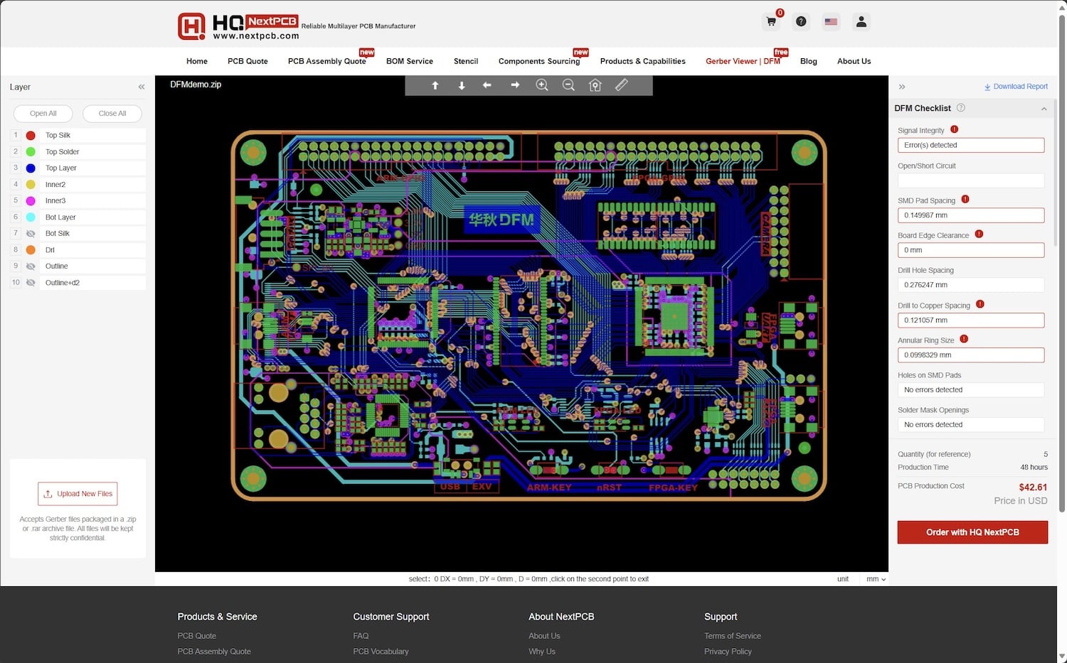
Figure 8. Screen view of the HQDFM DFM checker and Gerber viewing tool (click to enlarge).
Designed by the manufacturer, HQDFM from HQ NextPCB is a free tool for engineers to check for common Design for Manufacturing problems in their PCB Gerber files. The tool is based on real problems CAM engineers encounter on a daily basis. Engineers can also use it as a general-purpose Gerber Viewer to visualize their Gerber data. Download the HQDFM desktop suite to check for over 20 different DFM problems and get actionable insights or try the online Gerber Viewer version with a free DFM report.
Support With Gerber Files and PCB Manufacturing
No one wants the board design and layout process to adversely delay their product development. Since DFM review can be done at anytime, you can plan ahead and give your design a quick check while still finalizing your design. You don’t have to wait until you are ready to order and rely entirely on the fab house to report obvious problems. For additional support with Gerber files and your PCB manufacturing, contact HQ NextPCB.
Also, if you didn’t read the first two articles in this series and want to learn more, go check out the articles on Gerber file fundamentals and the details of Gerber layers for PCBs and stencils.
Featured image background used courtesy of Adobe
Industry Articles are a form of content that allows industry partners to share useful news, messages, and technology with All About Circuits readers in a way editorial content is not well suited to. All Industry Articles are subject to strict editorial guidelines with the intention of offering readers useful news, technical expertise, or stories. The viewpoints and opinions expressed in Industry Articles are those of the partner and not necessarily those of All About Circuits or its writers.


