Developing a Smart FPGA Power Solution: A Modular Approach
The task of powering FPGAs is full of complexities. Learn how a modular FPGA approach can enable you to meet tricky challenges including space constraints, voltage accuracy, power management, and integration.
This article is co-authored by Niliana Carrero, Applications Engineer at MPS
Powering field-programmable gate arrays (FPGAs) represents a challenge for power engineers due to their increasing number of logic cells, which increases complexity. In addition, these semiconductor devices are highly configurable, allowing designers to define the clock and phase-locked loop (PLL) frequencies, as well as configure the logic elements within them. Furthermore, defining the power consumption of an FPGA can be a complex task because it depends on factors such as the firmware, FPGA model, and operating conditions.
Most FPGA vendors provide power data that may include different power consumption targets for different conditions. That’s vital given that FPGAs are used in a wide variety of applications, including communications, industrial, automotive, and medical devices.
This article focuses on the FPGA power supply design for Intel (Altera) Agilex and how Monolithic Power Systems’ (MPS’s) fully integrated MPM3698 and MPM3699 modules help to minimize solution space while meeting one of the most challenging specifications: keeping the output voltage (VOUT) accuracy within 2% or 3% during very fast power transients.
FPGA Power Challenges
Efficient space utilization is a crucial aspect of designing FPGA that can impact cost, performance, and power consumption, making it a key consideration for power engineers and designers. Figure 1 shows the main challenges of FPGA power.

Figure 1. FPGA power challenges
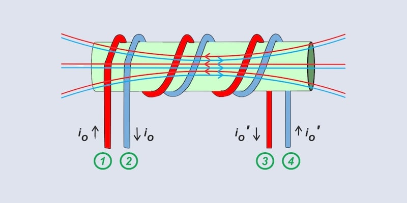
There are two main types of FPGA power supply rails: the core combined with a hard processor system (HPS), and transceivers. These distinct power domains within the FPGA have different design constraints; the core and HPS rails require stable accuracy across different loads and temperatures, while the noise-sensitive transceivers require their output to be below a certain noise level.
The next generation of FPGAs consists of multiple internal power domains that must start up or shut down in a specific sequence to ensure proper functionality. These internal power domains are divided into several groups.
Figure 2 shows the start-up and shutdown sequences of tree groups for Intel Agilex. Proper power sequencing helps prevent problems including voltage spikes, excessive current draw, unstable clocks leading to timing violations, and other electrical issues that can lead to damage or malfunction.
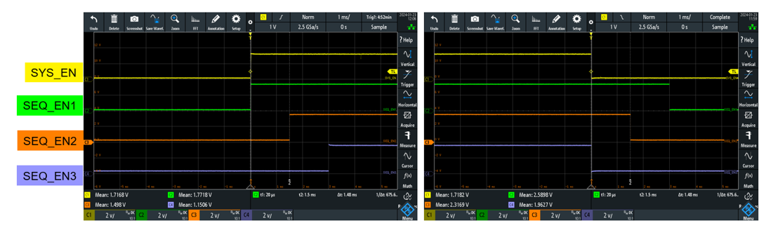
Figure 2. Start-up and shutdown sequences of tree groups for intel Agilex. (Click image to enlarge)
On the other hand, important considerations must be taken regarding the output voltage ripple (∆VOUT) or allowable variation from the nominal voltage specification, where most of the rails require VOUT accuracy within 2% or 3%. This is one of the most challenging FPGA design constraints, particularly in applications where the workload varies dynamically or when different parts of the device are activated or deactivated as necessary.
Excessive voltage ripple can lead to issues in FPGA operation, especially in sensitive analog or mixed-signal applications. Figure 3 shows a change in the load current without causing a significant deviation in VOUT (within the target ±3% tolerance).
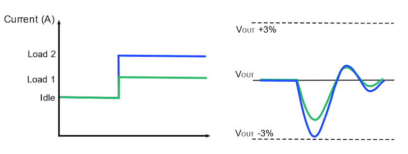
Figure 3. Output voltage ripple and dynamic power tolerances
VOUT is maintained within the target tolerance using the voltage controller circuits. These circuits adjust the voltage to meet the specified levels, preventing unwanted fluctuations that can affect the performance and reliability of the FPGA and connected components. It is essential to maintain the voltage level requirements of each FPGA’s rail within the specified tolerances for optimal performance. Furthermore, maintaining VOUT within the target tolerance ensures accurate signal processing as well as compatibility with other devices in the system.
Power Consumption Estimation
Workload variation is common in many FPGA applications, especially in fields such as telecommunications, software-defined radio (SDR), image processing, and edge computing. In these applications, the FPGA must adapt to changing data and processing requirements.
The most outstanding FPGA devices support dynamic reconfiguration, allowing the device’s functionality to be adjusted on the fly for multiple modes that are tailored to specific tasks. By understanding the workload variations, the complex task of estimating and measuring power consumption is simplified.
Power consumption estimation can span an iterative process that requires refinement as the design evolves. A detailed analysis often requires specific knowledge of the design’s functionality, resource utilization, and operational characteristics. This also includes understanding the amount of electrical current that an FPGA device may draw from its power supplies and distribute through its internal circuits.
The FPGA device’s electrical current can activate a significant number of logic elements by using high-speed I/O interfaces, driving external loads, or processing data-intensive workloads.
Considering All the Factors
Each of these factors can contribute to increased power consumption. In this scenario, it is essential to define the appropriate current for each rail when designing the board to ensure the safe, reliable FPGA operation. This may include selecting the appropriate voltage regulators, power sources, and power distribution networks to handle the current demands.
Most FPGA vendors offer tools to estimate the worst-case power consumption-based device utilization, which helps FPGA designers predict the power usage of their designs with reasonable accuracy. These tools also guide designers to make thermal management decisions for consistent FPGA operation without voltage fluctuations, overheating, or potential damage, and to meet the performance and power requirements. Overall, it is important to understand idle power, which is the leakage current when the device starts up, and the dynamic power resulting from the operating frequency.
Agilex Power Tree Using MPS Power Modules
A power tree is a graphical representation of the power management architecture. In this architecture, the input voltage (VIN) of the power supply transfer (typically between 4 V and 16 V) is converted to the voltage required by the FPGA, ensuring that each part of the device receives the required voltage and current. Figure 4 shows the Intel Agilex FPGA power tree with a complete MPS solution. Rail 1 uses the MPM3698 and MPM3699 modules, which can handle up to 200 A of current. This rail requires a nominal VOUT of 0.8 V, with a maximum tolerance of ±3% (DC + AC).

Figure 4. Intel Agilex power tree. (Click image to enlarge)
MPS’s fully integrated modules combine the controller, power stages, inductors, and most passive elements into a single package. This layout is optimized to reduce circuit parasitic inductance and capacitance, improve thermally efficient connectivity to the PCB, and increase overall system efficiency.
In addition, MPS power modules offer fault protections such as over-voltage protection (OVP), under-voltage protection (UVP), thermal shutdown, along with power-saving techniques including active voltage positioning (AVP), automatic phase-shedding, and the voltage identification (VID) code function. All of the MPM3698’s features are fully supported by MPS’s Virtual Bench Pro 4.0 software, which helps users configure the device based on different system requirements.
Consolidating Components
Power modules streamline power supply design by consolidating various components, including voltage regulators, inductors, and capacitors into a single module. The integrated design minimizes the discrete component count and accelerates the overall design process, simplifying the selection of input and output capacitors on the PCB and enhancing the overall efficiency of the power supply design.
As a result, only the input and output capacitors need to be selected on the PCB to complete the full power module design. This enables designers to develop new applications in a short period with the benefits of digital control and sequencing.
Furthermore, power modules are easy to integrate into the circuit, as they are available in standard packages with common pinouts and their compact design makes them ideal for space-constrained applications. These modules are commonly used in various applications, including power supplies for FPGAs, microcontrollers, and other electronic devices. Figure 5 shows an example of a module layout using high-precision passive components.

Figure 5. Fully integrated module layout
Power Supply Design for Fast Power Transients
The flexibility and configurability of FPGAs must be matched by their power supplies to meet the dynamic power requirements of these devices. Adaptability is at a premium in applications where FPGA configurations and modes frequently change.
The MPM3698 and MPM3699 are fully integrated MPS power modules for FPGAs that offer a sophisticated power supply solution combining two main communication protocols: PMBus and AVSBus.
The PMBus protocol allows real-time monitoring of power supply parameters, such as voltage, current, and temperature. It enables digital control loop configuration to meet FPGAs’ strict voltage regulation, with the ability to tune the feedback loop during aggressive load steps.
PMBus also enables Intel Smart Voltage IDentification (SmartVID), a power optimization technique that compensates for the process variation by using adaptive voltage scaling with PMBus. This technique saves power to optimize energy efficiency and performance. Figure 6 shows the general configuration for the SmartVID controller across a VCC rail.

Figure 6. Intel SmartVID Is enabled using PMBus
In our implementation, we use the Intel FPGA Power and Thermal Calculator to estimate the power for the Intel Agilex core voltage (VCC) and peripheral voltage (VCCP). The step load is calculated as follows: 80% of core utilization, 80% of digital signal processor (DSP) utilization, and 30% of M20K memory block utilization, with the toggling rate assumed to be 15%.
Table 1 shows the initial step load and slew rate under the estimated conditions.

Table 1. Step load specification for the VCC and VCCP core
Furthermore, the EVINAG-001-A FPGA evaluation board from the Intel Agilex reference design can be used to evaluate the performance of the MPS power modules and check that the specifications from Table 1 are obtained (see Figure 7).
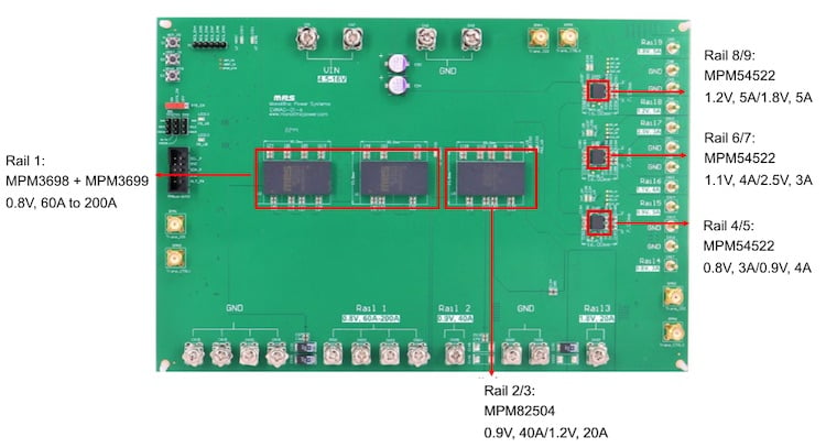
Figure 7. EVINAG-001-A FPGA evaluation board for Intel Agilex
Figure 8 shows the load transient response and ripple measurement for the VCC/VCCP core rails using the specifications given in Table 1. The total required output capacitors are 32 x 47 μF multilayer ceramic capacitors (MLCCs) and 4 x 330 μF polymer capacitors (POSCAPs).
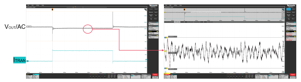
Figure 8. Load transient of the MPM3698 and MPM3699 using the EVINAG-001-A FPGA evaluation board (VCC/VCCP Core Rail with ∆IOUT = 32.5 A, Slew Rate = 325 A/μs, VIN = 12V, VOUT = 0.8 V, and fSW = 500 kHz). (Click image to enlarge)
In Figure 8, the peak-to-peak VOUT during load transient is 228.1 mV and the output ripple measurement at heavy load currents (right waveform) is 12.264 mV. This is within the ±3% maximum VOUT tolerance (DC + AC). Refer to the EVINAG-01-A Test Report for additional measurements for the Intel Agilex FPGA power tree with the complete MPS module solution under different load step specifications.
Output Capacitance Design Guidelines
Maintaining a stable power supply during dynamic changes in power consumption is crucial for reliable and consistent FPGA operation. Many factors impact achieving a stable power supply; while optimizing the control loop’s behavior during load transients ensures that the power supply’s VOUT remains within specified tolerances, the proper selection of the bypass and decoupling capacitors also plays a significant role in keeping VOUT constant.
Particularly in high-speed, high-density PCB designs, small improvements in the decoupling network can have a significant impact on the FPGA’s overall performance and signal integrity. Decoupling capacitors should be strategically placed throughout the PCB layout to effectively filter and decouple power and ground connections.
Additionally, every core BGA pin requires a direct connection to high-quality ceramic capacitors. Although traditional design guidelines recommend placing the decoupling capacitors on the bottom side of the PCB, it is essential to understand the tradeoffs and considerations involved. Integrating additional parts in space-constrained areas requires allocating capacitors to share the same vias.
The parasitic elements of the vias (for example, inductance and resistance) can impact the effectiveness of the decoupling network, and there are scenarios where sharing vias may have an impact on overall performance. Figure 9 shows the recommended capacitor layout for the FPGA design.
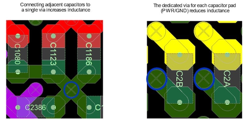
Figure 9. Recommended capacitor layout for the FPGA design
Many Benefits to the Modular Approach
The evolution of FPGA typically follows trends of increasing density and performance while reducing power consumption and space requirements. In severely space-constrained FPGA applications, compact power modules can provide a valuable solution to save space and minimize the risk of parasitic elements affecting the power distribution network (PDN).
Although compact power modules may have a slightly higher unit cost compared to discrete components, they can ultimately lead to cost savings by reducing the component count, assembly time, and the risk of design errors, which is particularly advantageous for rapid prototyping and production efficiency.
This article presented a power module for FPGA solution with the MPM3698 and MPM3699 that reduces the layout and optimizes passive components, which boosts EMI performance due to the smaller loops of the package. The solution provides a stable and allowable VOUT tolerance, as well as clean power to the FPGA during very fast power transients. Explore the full range of MPS’s step-down power modules to discover the best option for your smart FPGA power solutions.
All images used courtesy of Monolithic Power Systems (MPS)
Industry Articles are a form of content that allows industry partners to share useful news, messages, and technology with All About Circuits readers in a way editorial content is not well suited to. All Industry Articles are subject to strict editorial guidelines with the intention of offering readers useful news, technical expertise, or stories. The viewpoints and opinions expressed in Industry Articles are those of the partner and not necessarily those of All About Circuits or its writers.