Facebook
 Google
 GitHub
 Linkedin
Automated 3D Reconstruction: How Chipmakers Can Keep Pace in the AI Era
As chipmakers stack dies vertically to meet surging AI demand, 2D imaging is losing its edge. Automated 3D reconstruction is becoming essential to keeping fabs on pace.
The semiconductor chips powering today’s AI infrastructure are made with increasingly complex geometries. As semiconductor manufacturers look to meet surging data center demand, the industry has pivoted to 3D stacking architectures to create chips that boost bandwidth and improve energy efficiency. From nanometer-scale transistor structures to multi-die high-bandwidth memory (HBM) assemblies approaching millimeter dimensions, the industry has gone vertical across nearly every length scale to increase chip performance. However, this structural leap to 3D introduces new defect analysis challenges that 2D imaging solutions struggle to solve.
This shift directly impacts work in the lab and on the fabrication floor. As vertical integration continues, buried defects become harder to find. The limitations of 2D imaging can result in ambiguous results when trying to fully characterize complex 3D structures. The result is a slower time to root cause determination and repeated analysis cycles. At the same time, fabs want to move faster to meet increasing demand. When analysis in the lab lags, it creates a significant gap between the two functions that creates risk for ramp and yield.
Adopting automated 3D reconstruction and precise 2D planar imaging from any desired orientation are the practical paths to closing this gap. With these technologies, semiconductor manufacturers can separate buried defects from surface signals, visualize the geometry of defects across layers, and increase throughput. As semiconductors become more complex, these workflow enhancements are shifting from specialized techniques to production requirements.
Turning to 3D Stacking Architectures for More Energy-Efficient Semiconductor Chip Production
The World Semiconductor Trade Statistics organization forecasts that global semiconductor sales will reach approximately $1.5 trillion in 2026, with memory projected to account for more than $800 billion of that total. Due to this projected growth and increasing memory demands, semiconductor manufacturers must continue to evolve advanced packaging technologies. This includes using 3D stacking architectures to meet rising performance, density, and scalability requirements. 3D stacking architectures involve placing multiple layers of silicon on top of one another rather than laying them flat. This reduces the distance data must travel, resulting in faster, more energy-efficient, and more compact chips. Multiple dies must work perfectly together, with each die meeting a high yield threshold. If even one layer falls short, it degrades the yield of the entire stack.
Leveraging known-good die (KGD) screening for viable HBM can help ensure each die is complementary and is produced at a higher quality. The performance gains are measurable. In fact, the benefits of 3D stacking are evident in one use case: 3D buffer memory. According to IMEC, 3D buffer memory is projected to provide five times more bit density than dynamic random-access memory (DRAM) is expected to offer by 2030,
HBM is already central to the growing AI ecosystem and perhaps one of the most visible examples of 3D stacking going mainstream. As advanced technology from AI to wireless continues to drive demand, manufacturers must engage in more stacking to meet performance targets.
Without scalable 3D analysis capabilities, semiconductor manufacturers are at risk of slower yield learning, more rework loops, and false confidence due to incomplete 2D evidence. This highlights a critical need for imaging technology that produces clearer, higher-quality images that can help manufacturers catch defects early in the process. Semiconductor manufacturers can meet this need by leveraging advanced imaging technologies like scanning electron microscopes (SEMs) and focused ion beam (FIB) systems.
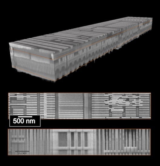
As lateral scaling reaches its limits, both logic and DRAM are increasingly scaling in the vertical dimension. Logic is progressing from FinFET to GAA to CFET, while DRAM structures are becoming increasingly 3D to improve bit density and capacitor scaling. This shift creates a growing challenge for traditional 2D failure analysis, as critical structures become both more complex in 3D and significantly smaller than those in advanced packaging.
3D analysis of logic samples down to the single nanometer scale. Image used courtesy of Thermo Fisher Scientific
Clarifying Signals With 3D Reconstruction
The core limitation of 2D imaging for defect analysis is dimensionality and the precision of positioning the 2D plane with respect to the region of interest. When electron-beam-based imaging captures a signal from a 2D cross-section, it collapses the subsurface features into a single plane. With voids, delaminations, and cracks appearing across the multiple layers within the chip, the images can be difficult to interpret accurately.
This then leads to various back-and-forth conversations between the failure analysis and processing teams, delaying root cause determination and slowing corrective actions. Furthermore, 2D imaging is only acceptable if the plane of imaging is correctly positioned to capture the failure or region of interest.
Alternatively, 3D imaging methods provide a more complete view of defects across chip layers, promoting easier and more consistent interpretation. In fact, advanced 3D imaging methods have shown five times the gains in defect sensitivity compared to 2D, according to NIST. 3D imaging can make it easier to determine where voids propagate, whether they interconnect across layers, and their relationship to similar features.
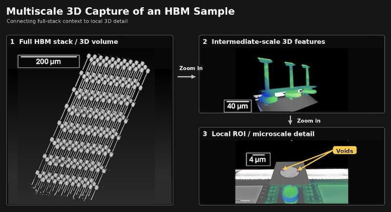
A key challenge when imaging advanced packaging for failure analysis is finding a small defect in a large volume, which requires bridging many length scales in 3D or precision targeting in 2D. Similarly, the direction and growth of cracks through interfaces are much clearer with 3D imaging. By producing consistent 3D imaging evidence, semiconductor manufacturers can make decisions faster and with more confidence.
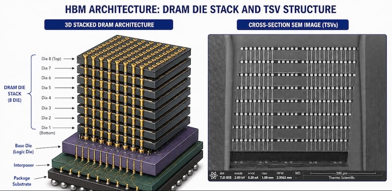
Precision 2D cross-sectioning targets features deep below the surface—TSVs under 5 µm in diameter, bisected across the entire DRAM stack. Image used courtesy of Thermo Fisher Scientific
If 2D imaging is the only pathway, then the analysis tool must be precise enough to capture the correct imaging plane in the exact orientation. This may become tricky when the user needs to find small features or defects across a large imaging plane.
3D imaging across length scales, allowing the user to zoom in on a small feature in a large volume. Image used courtesy of Thermo Fisher Scientific
Overcoming the Throughput Constraints With 3D
The benefits of leveraging 3D imaging technology are clear. You receive more confident results earlier. However, one main hurdle remains: throughput constraints. The time it takes to integrate 3D imaging must not outweigh the increased resolution and quality that the technology provides.
By leveraging automation alongside 3D imaging, manufacturers can alleviate these throughput constraints. Automation has the power to shorten time-to-yield and improve throughput by removing manual bottlenecks, flagging defects earlier, and optimizing complex, multi-step processes. It can also help manufacturers engage in smarter KGD screening by running high-throughput automated wafer probing, which can result in fewer bad dies that enter the stack.
Increasingly, semiconductor manufacturers are combining AI and automation with 3D imaging to overcome these time constraints, which is a natural evolution given the pressure to deliver accurate results faster without sacrificing quality.
Shifting to 3D Stacking Architectures
The demand for smaller and more complex chips, led by the increased use of advanced technology, like AI and wireless, presents a clear pathway for integrating 3D imaging into the semiconductor lab and fab. Automated 3D reconstruction and metrology enable better quality results and, though the results may take longer to produce, they are clearer and support more confident decision-making. 3D analysis is a competitive advantage that semiconductor manufacturers must look to integrate into their workflows, particularly as AI and similar technologies become more widely adopted.
For 3D imaging to become an industry standard, companies must invest deliberately in the technology and workflows. Semiconductor manufacturers that act now will be best positioned to meet the demands of an increasingly complex, AI-driven industry.
Related Content